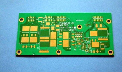
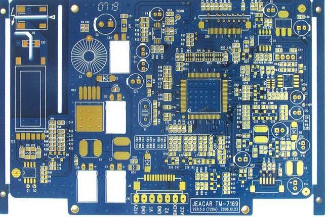
Application of PCB interconnection technology-basic knowledge

1 Traditional plated through holes
The most common and cheapest interlayer interconnection technology is the traditional plated through hole technology. In this technology, all holes are drilled through the panel, regardless of whether they are applied like component holes or via holes. The main disadvantage of this technology is that the vias take up precious space in all layers, regardless of whether the layer needs to be electrically connected.
2 Buried hole
Buried holes are plated through holes that connect two or more layers of multiple substrates. The buried holes are in the inner structure of the circuit board and do not appear on the outer surface of the circuit board. Compared with the traditional plated through hole structure, the buried hole saves a lot of space. When the signal line density is high, more holes are needed to connect to the signal layer, and more signal routing paths are needed, buried via technology can be used. However, because the buried via technology requires more process steps, the advantage of the circuit density is to increase the cost of the circuit board.
3 blind holes
Blind vias are plated through holes that connect the surface of a multi-substrate to one or more layers, and they do not pass through the entire thickness of the board. Blind holes can be used on both sides of a multi-substrate. Blind holes can connect via holes and component holes passing through the PCB circuit board. Blind vias can be stacked on top of each other and can be made smaller, which can provide more space or route more signal lines.
For SMD and connectors, blind via technology is particularly useful because they do not require large component holes, only small vias to connect the outer surface to the inner layer. On very dense and thick multi-substrates, the use of surface mount technology can reduce weight and provide designers with sufficient design space.
The above is about the application of PCB interconnection technology-basic knowledge introduction, Ipcb also provides PCB manufacturers and PCB manufacturing technology.