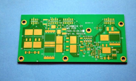
In today's industry, system printed circuit boards layout has become an integral part of the design itself. Therefore, design engineers must understand the mechanisms that influence the design performance of high-speed signal chains.
In high-speed analog signal chain design, the layout of printed circuit boards (PCBS) requires consideration of many options, some more important than others, and some depending on the application. The final answer varies, but in all cases design engineers should try to eliminate the error of best practice without obsess over every detail of layout and wiring. The information provided in this application note will be helpful to design engineers for their next high speed design project.

Bare solder
Bare pads (EPAD) are sometimes overlooked, but they are important to maximize the performance of the signal chain and to maximize the heat dissipation of the device.
The bare pad, which ADI calls pin 0, is the pad underneath most devices today. It is an important connection through which all the internal grounding of the chip is connected to a central point below the device. Have you noticed that many converters and amplifiers are currently missing ground pins because of bare pads?
The key is to properly fix (weld) this pin to the PCB for a strong electrical and thermal connection. If this connection is not strong, confusion occurs, in other words, the design may not work.
Achieve optimal connection
There are three steps to achieving optimal electrical and thermal connections with bare pads. First, where possible, bare pads should be duplicated on each PCB layer in order to form dense thermal connections with all ground and ground layers for rapid heat dissipation. This step is relevant for high-power devices and applications with high channel numbers. On the electrical side, this will provide a good equipotential connection for all the ground layers.
The bare pad can even be duplicated on the bottom layer (see Figure 1), which can be used as a decoupling heat sink ground point and a place to install the bottom side radiator.
For example, when a circuit board is unable to achieve good layout segmentation due to size constraints, the grounding layer needs to be separated. This may be because dirty bus power supplies or high-noise digital circuits must be placed in certain areas to meet traditional design requirements or dimensions. In this case, separating the formation is the key to achieving good performance. However, for the overall design to be effective, these grounding layers must be connected together by a bridge or connection point somewhere on the circuit board. Therefore, the joint points should be evenly distributed over the separated grounding strata.
Eventually, there is often a connection point on the PCB that is the best place for the return current to pass through without degrading performance or forcing the return current to be coupled to the sensitive circuit. If this connection point is located near, or below the converter, no separate grounding is required.
conclusion
Layout considerations are always confusing due to the plethora of optimal options. Technology and principles have always been part of the company's design culture. Engineers like to learn from previous designs, and the pressure to get to market makes designers reluctant to change or try new technologies. They are stuck in risk balancing until there is a major problem in the system.
At the evaluation board, module, and system levels, a simple single grounding is best. Good circuit segmentation is the key. This also affects the layout of layers and adjacent layers. If the sensitive layer is above the high-noise digital layer, be aware that cross coupling may occur. Assembly is also important; Manufacturing notes provided to PCB shop or assembly shop should be used to ensure a reliable connection between IC bare pad and PCB.
Poor assembly often results in poor system performance. Decoupling of VDD pins near the power layer entry point and the converter or IC is always advantageous. However, to increase the inherent high-frequency decoupling capacitance, tightly stacked power supplies and grounding layers should be used (spacing ≤4 mils). This method comes with no extra cost and only takes a few minutes to update the PCB manufacturing notes.
When designing a high-speed, high-resolution converter layout, it is difficult to take all the specific features into account. Each application is unique. It is hoped that the points described in this application note will help design engineers better understand future system design.