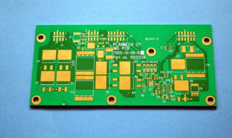
In PCBA mounting, after the PCB board is wave soldered, the solder mask on the board can not withstand the "test of love" with the circuit board, causing the boat of friendship to turn upside down.

Below, we will discuss the reasons for their "parting ways" with your friends in simple and simple language.
If the two-phase molecules of the ink and the PCB substrate have a strong opposite polarity, it will produce gravitational force, which is called secondary bonding force. The ink and the substrate are attached together due to the secondary bonding force, which is called secondary bonding. Combine.
Because the opposite sex attracted each other, the two "people" had a spark of love. This is the reason why they "come together" in the first place.
After undergoing the high temperature test of wave soldering, the secondary bonding force of the solder mask ink and the copper layer decreased, the thermal shock resistance was poor, and the solder mask film fell off.
The main reasons that affect the bonding force of the printed board and the solder mask ink are as follows:
1. The quality of solder mask ink
Poor quality of solder mask ink, improper preparation, use beyond the shelf life, or improper blending during preparation, will result in poor thermal shock resistance and easy peeling of the solder mask.
2. Poor surface treatment of printed board before solder mask
The surface of the PCB printed board is poorly treated before the solder mask or the solder mask is left for a long time after the treatment. The oxide layer, water marks or stains on the surface of the printed board will affect the bonding force of the solder mask. In the subsequent high temperature impact, due to the large difference in thermal expansion coefficient between the solder mask and the metal copper layer, thermal stress is generated and the solder mask falls off.
If there is a slight change in the color of the copper layer after the solder mask is peeled off, it means that the part of the printed board that has fallen off has a poor surface treatment.
3.3 Solder mask thickness
The adhesion of solder mask at high temperature is closely related to its thickness. Under the premise of thorough curing, the greater the thickness within a certain range, the stronger its thermal shock resistance.
This is the reason why the two "people" could not withstand the temptation of feasting or the test of life, and their will was not strong, which resulted in the separation.
So how can we make their "love" last longer, and the sea will die? !
1. Ink quality requirements
Solder mask printing must have good film-forming properties and meet the requirements of IPC-840C and IPC-A-600E.
2. Control the pre-treatment of solder mask to ensure the quality of pre-treatment
The pre-treatment of solder mask is very important, especially the effect of cleaning and roughening the copper surface, which has a great influence on adhesion. Therefore, the pre-treatment must require the PCB surface to be clean and have a good surface roughness to ensure good adhesion between the ink and the surface.
3. Post curing control
If the post-curing temperature is not enough, the ink will not be cross-linked completely, and the solder mask will not be able to withstand the thermal shock of high temperature well. If the curing temperature is too high, the ink will be embrittled. Therefore, a curing temperature and time must be selected according to the process requirements of the ink.
At the same time, note that after the ink is printed, it is best to stand for a while to eliminate the tiny bubbles generated by the ink during printing and enhance the adhesion to the board surface.
In addition, the temperature in the box should not be too high, and the hot air circulation in the box must be good, and the temperature uniformity in the box must meet the requirements. Because if it enters the tank, it will be high temperature. A hard film will quickly form on the surface of the oil layer to cover the entire oil layer. The solvent inside cannot overflow, and the solvent stays in the oil layer. If the oil explodes and the air is not well ventilated in the box, it will cause the solvent to linger in the box and cause poor curing.
4.4 Control of ink thickness
The solder mask, especially the solder mask at the edge of the line, is not thick enough, which reduces the bonding force between the solder mask and the copper layer, and will fall off after the high temperature impact of subsequent wave soldering.
The mesh number and tension of the screen, the ratio of the ink and the hardness, pressure, speed, and angle of attack of the squeegee all have a close relationship with the thickness. In daily work, it is necessary to find a better combination of process parameters according to the specific conditions.
The ink thickness of the second squeegee is thicker than that of the first squeegee, but the increase in the number of squeegees does not contribute much to the thickness. The advantage of the second squeegee is to improve the uniformity of the ink, especially the back and forth printing in different directions, which is beneficial to prevent the jump printing at dense lines and higher lines, and has a good guarantee for the thickness of the solder mask at the edge of the line.
In short, the peeling of the solder mask is due to the low bonding force between the solder mask and the copper layer. In the subsequent high temperature impact, due to the large difference in thermal expansion coefficient between the solder mask and the metal copper layer, thermal stress causes the solder mask to fall off .
The main reasons that affect the bonding force of the solder mask of the printed board are: poor surface treatment of the printed board, poor quality or improper preparation of the solder mask, and insufficient thickness of the solder mask.
The production process of liquid solder mask is more complicated. Only by finding a strong PCB manufacturer and strengthening the control and monitoring of the production process can the defects of solder mask be effectively avoided, so that their "love" will last longer and be able to withstand it. The severe test of all kinds of ups and downs.