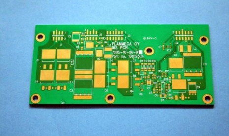
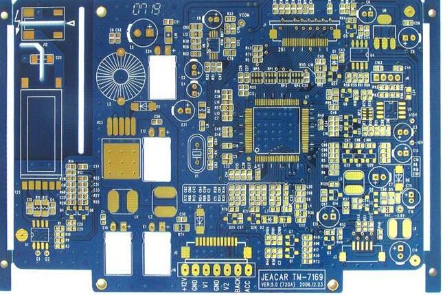
Many people may not pay much attention to the solder mask on the PCB circuit board, thinking that it may be a thin film on the circuit board, which is not very useful, and the quality and coating material are just fine. In fact, the PCB solder mask is also an extremely important part of the circuit board, which plays a decisive role in the circuit board.

As the name implies, preventing short circuits between PCB solder joints, pads, and circuits is the first function of the PCB solder mask. In addition, it is also a layer of protective armor that the circuit board "wears" on the body, which has the functions of anti-oxidation, anti-corrosion, anti-pollution, and anti-moisture.
Let's take a look at several common defects of solder mask and precautions for production.
1. Skip printing phenomenon of PCB solder mask
Target conditions-Level 3, 2, 1
• The solder mask has a uniform appearance on the surface of the substrate, the sides of the conductor and the edges, and has been firmly bonded to the surface of the printed board, without visible jump prints, voids or other defects.
Acceptable conditions-level 3,2
• In areas where there are parallel conductors, except for areas where the solder mask is deliberately not covered between the conductors, no adjacent conductors are exposed due to the lack of solder mask.
• If it is required to repair with solder mask to cover these areas, use a material that is compatible with the solder mask originally used and has the same resistance to soldering and cleaning.
Acceptable conditions-level 1
• The missing solder mask did not reduce the spacing between conductors below the minimum acceptability requirement.
• There may be a solder mask with jump prints along the sides of the conductive pattern.
Not eligible-level 3, 2, 1
• The defect does not meet or exceed the above requirements.
2. The degree of coincidence with the hole (all coating layers)
Target conditions-Level 3, 2, 1
• There is no dislocation of the solder mask. The solder mask is within the nominal coincidence pitch and surrounds it with the connecting pad as the center.
Acceptable conditions-level 3, 2, 1
• The solder mask pattern is misaligned with the connection pad, but it does not violate the minimum ring width requirement.
• Except for those holes that do not need to be soldered, there is no solder mask in the plated holes.
• Adjacent lands or conductors that are electrically isolated from each other are not exposed.
Not eligible-level 3, 2, 1
• The defect does not meet or exceed the above requirements.
3. The degree of coincidence with the rectangular surface mounting connection plate
Target conditions-Level 3, 2, 1
• There is no dislocation of the solder mask.
Acceptable conditions-level 3, 2, 1
• The misalignment between the solder mask and the lands defined by the copper foil does not expose adjacent electrically isolated lands or conductors.
• The solder mask does not encroach on the printed contacts or test points on the edge of the board.
• For surface mount lands with a pitch greater than 1.25 mm [0.050 in], only one side of the lands can be invaded, and no more than 50 μm [1,969 μin].
• For surface mount lands with a pitch between 0.65 mm [0.0256 in] and 1.25 mm [0.050in], only one side of the lands can be invaded, and no more than 25 μm [984 μin].
• For surface mount lands with a pitch of less than 0.65 mm [0.0256 in], the value of invading lands needs to be negotiated between the supplier and the buyer (AABUS).
Not eligible-level 3, 2, 1
• The defect does not meet or exceed the above requirements.
3.1 The degree of coincidence with the circular surface mount land (BGA)-the land defined by the solder mask
The solder resist film defines the connection pad: a part of the conductive pattern in the PCB, which is used to connect the ball terminals of electronic components (BGA, fine pitch BGA, etc.). The solder mask occupies the edge of the connection pad, thereby limiting the spherical connection to the resistance The soldering film surrounds the range.
Target conditions-Level 3, 2, 1
• The overlap area between the solder mask and the connection pad is centered around the connection pad.
3.2 Coincidence degree with round surface mount land (BGA)-land limited by copper foil
The connection pad defined by the copper foil: usually (but not necessarily) part of the conductive pattern. During the welding process, the connection pad metal is used to connect and/or solder the components. If the product is coated with a solder mask, leave around the connection pad There are gaps.
Target conditions-Level 3, 2, 1
• The solder mask is centered around the copper connection pad, and there is a gap around it.
Acceptable conditions-level 3, 2, 1
• Except for the conductor connection, the solder mask is uncoated and occupies the connection pad.
Not eligible-level 3, 2, 1
• The defect does not meet or exceed the above requirements.
3.3 Coincidence degree with the circular surface connection plate (BGA)-(welding resistance dam)
Solder mask dam: A part of the solder mask pattern used for BGA or fine pitch BGA mounting connections. A small piece of solder mask material separates the mounting part of the pattern from the interconnect vias to prevent solder from falling into the soldering place In the via hole.
Target conditions-Level 3, 2, 1
• The solder mask is centered on the copper connection pad and the via hole, and there is a gap. The solder mask only covers the conductors between the copper lands and the vias.
4. Foaming/Laminating
Target conditions-Level 3, 2, 1
• There is no sign of adhesion, delamination or blistering between the solder mask and the printed board substrate and conductive patterns.
Acceptable conditions-level 3,2
• There can be two flaws on each side of the printed board, and the maximum size of each flaw does not exceed 250 μm [9,843 μin].
• The reduction in electrical spacing due to blistering or delamination does not exceed 25% of the spacing, or the minimum spacing.
Acceptable conditions-level 1
• Blistering or delamination does not bridge the conductors.
Not eligible-level 3, 2, 1
• The defect does not meet or exceed the above requirements.
5. Adhesion (peeling or peeling)
Target conditions-Level 3, 2, 1
• The surface of the solder mask has a uniform appearance and firmly adheres to the surface of the printed board.
Acceptable conditions-level 3,2
• There is no sign of solder mask lifting from the board before the test.
• When the design requires the edge of the printed board to be covered with solder mask, the chipping or floating of the solder mask on the edge of the printed board cannot penetrate more than 1.25 mm [0.050 in] or 50% of the distance from the nearest conductor, whichever is more Small value.
• After testing in accordance with IPC-TM-650 test method 2.4.28.1, the amount of solder mask falling off does not exceed the allowable limit specified in the IPC-6010 series of standards.
Acceptable conditions-level 1
• Before the test, the solder mask peeled off from the printed board substrate or conductive pattern surface, but the remaining solder mask was firmly adhered to the board surface. The missing solder mask did not expose the adjacent conductive patterns or did not exceed the allowable value for peeling off.
• When the design requires the edge of the printed board to be covered with solder mask, the chipping or floating of the solder mask on the edge of the printed board cannot penetrate more than 1.25 mm [0.050 in] or 50% of the distance from the nearest conductor, whichever is more Small value. • After testing in accordance with IPC-TM-650 test method 2.4.28.1, the amount of solder mask falling off does not exceed the allowable limit of the IPC-6010 series of standards.
Not eligible-level 3, 2, 1
• The defect does not meet or exceed the above requirements
6, ripples/folds/wrinkles
Target conditions-Level 3, 2, 1
• There are no wrinkles, ripples, wrinkles or other defects on the surface of the printed board substrate or the solder mask coating on the conductive pattern.
Acceptable conditions-level 3, 2, 1
• The ripples or wrinkles in the solder mask did not reduce the coating thickness of the solder mask below the minimum thickness requirement (when specified).
• The wrinkles that appear in an area do not bridge the conductive pattern, and meet the requirements for solder mask adhesion in the IPC-6010 series of performance specifications.
Not eligible-level 3, 2, 1
• The defect does not meet or exceed the above requirements.
7. Masking (vias)
The mask material is used to coat the hole, and there is no via hole of other additional material in the hole. The material can be applied from either side or both sides of the via, but it is not recommended to mask the via from one side.
Target conditions-Level 3, 2, 1
• All holes required to be masked are completely covered by the mask.
Acceptable conditions-level 3, 2, 1
• All holes required to be masked are completely covered by the mask.
Not eligible-level 3, 2, 1
• The defect does not meet or exceed the above requirements.
8. Suction tube gap
Suction tube void: An elongated tubular void along the edge of the conductive pattern, that is, the solder mask is not bonded to the surface of the substrate or the edge of the conductor. Tin/lead hot-melt flux, hot-melt oil, soldering flux, cleaning agent or volatiles may be trapped in this suction tube void.
The above is an introduction to the problem of PCB solder mask. Ipcb is also provided to PCB manufacturers and PCB manufacturing technology.