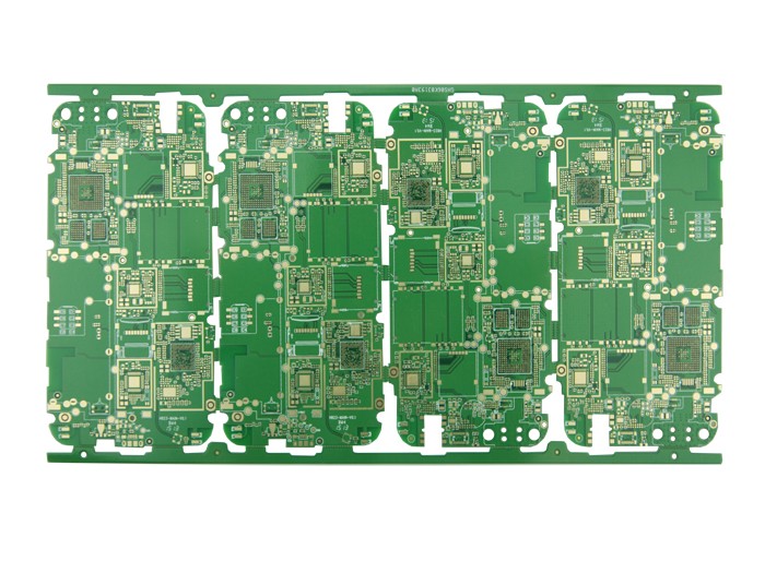
(1) PCB circuit board wiring design principles

1. Leads should avoid sharp and right-angle wiring. It is advisable to use 45° wiring.
2. The adjacent layer signal lines are orthogonal.
3. The signal in the high frequency PCB circuit board should be as short as possible.
4. Input and output signals should try to avoid adjacent parallel wiring, and it is best to add a ground wire in the middle of the circuit to prevent feedback coupling.
5. The direction of the power line and ground line of the double-layer PCB board should be consistent with the data flow direction to enhance the anti-noise ability of the PCB board.
6. Digital ground and analog ground should be separated. For low-frequency circuit PCBs, single-point parallel grounding should be used as much as possible;high-frequency PCB circuit boards should be multi-point series grounding (this is covered in the previous series of PCB design articles, there is a need Friends of you can refer back to related articles). For digital circuits, the ground wire should be closed into a loop to improve the anti-noise capability of the board.
7. For clock lines and high-frequency signal lines, the line width should be considered according to their characteristic impedance requirements to achieve impedance matching.
8. The wiring and perforation of the whole circuit board should be even to avoid obvious uneven density. When the outer signal of the printed circuit board has a large blank area, auxiliary wires should be added to make the distribution of the metal wires on the board basically balanced.
(2) Process requirements for wiring design
1. Below, our company’s big guys have listed the most commonly used trace widths and via sizes for wiring:
Note: The via hole under the BGA package component needs to be plugged with resin on both the front and back sides according to the requirements of the processing technology.
1) When the trace width is 0.3mm
When the PCB trace width is 0.3mm, the recommended size of each element
2) When the trace width is 0.2mm:
When the line width is 0.3mm, each element size recommendation table
3) When the trace width is 0.15mm
When the PCB line width is 0.15mm, the recommended size of each element
4) When the trace width is 0.12mm
When the PCB line width is 0.12mm, the recommended size of each element
Warm reminder, the distance between the pads under the BGA and the via pads between the pads is also the line width. And due to process reasons, it is not recommended to use a line width of 0.12mm.
Recommended size of via pads
5) When the line width is less than or equal to 0.12mm, the via pad needs to be added with teardrops. T in the table means that the teardrop needs to be added. When the size of the board is larger than 600mm, the width of the via pad needs to be increased by 0.1mm. Unit in the table: mm
Standard pad size table
For non-porous holes, the solder resist window diameter (the solder resist window) should be 0.50mm larger than the hole diameter. The width of the surface isolation zone is also determined by the size of the hole. When the diameter of the hole is less than or equal to 3.3mm, the range is "aperture + 2.0"; when the diameter of the hole is greater than 3.3mm, the range is 1.6 times the aperture. The range of the inner isolation zone is "aperture +2.0mm"
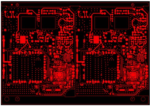
2. Specific PCB wiring principles:
1) Wiring of power supply and ground
Try to provide a separate power layer and bottom layer; even if you want to pull the wire on the surface layer, the power wire and ground wire should be as short as possible and thick enough.
For multi-layer PCB circuit boards, there are generally power planes and ground planes. Note that the ground and power supply of the analog part and the digital part must be separated even if the voltage is the same.
For single and double-layer PCB boards, the power cord should be as thick and short as possible. The width requirements of the power line and the ground line can be calculated based on the 1mm line width corresponding to the maximum current of 1A, and the loop formed by the power line and the ground should be as small as possible.
For single and double-layer PCB board power lines and ground lines constitute a design recommendation diagram
In order to prevent the coupling noise on the power line from directly entering the load device when the power line is long, the power supply should be decoupled before entering each device. And in order to prevent them from interfering with each other, the power supply of each load is independently decoupled and filtered before entering the load.
2) Special signal wire wiring
A. The wiring of the clock:
The clock line is one of the factors that have the greatest impact on EMC. Make fewer holes in the clock line, try to avoid running the line with other signal lines, and keep it away from the general signal line to avoid interference to the signal line. At the same time, avoid the power supply part on the PCB board to prevent the power supply and the clock from interfering with each other.
When multiple clocks of different frequencies are used on a circuit board, two clock lines of different frequencies cannot run side by side. At the same time, the clock line should also try to avoid being close to the output interface to prevent high-frequency clocks from being coupled to the output cable line and emitted along the line.
If there is a dedicated clock generating chip on the board, it cannot be routed underneath it, copper should be laid under it, and the ground can be specially cut off if necessary.
For crystal oscillators that many chips have reference, wires can also be routed under these crystal oscillators, and copper should be laid for isolation. At the same time, the crystal housing should be grounded.
For a simple single and double-layer PCB board, there is no power layer and ground layer, and the clock trace can be seen in the figure below
Single and double-layer PCB board clock routing reference diagram
B. Paired differential signal line routing
Differential signal lines appearing in pairs are generally routed in parallel, with as few holes as possible. When holes are required, the two lines should be punched together to achieve impedance matching.
C. A group of buses with the same attribute should be routed side by side as much as possible, and the length should be as equal as possible.
D. Some basic PCB wiring principles.
Considering heat dissipation, avoiding continuous welding and other factors, try to use Good lay-out as shown in the figure below to avoid bad lay-out.
When the distance between two solder joints is very small (such as the adjacent pads of SMD devices), the solder joints must not be directly connected.
The distance between the two solder joints of the PCB is very small, and the solder joints must not be directly connected.
The vias leading from the PCB patch pad should be as far away as possible from the pad.
The vias drawn from the PCB patch pad should be as far away as possible from the pad
3) Addition of copper coating
The inner layer of the multi-layer PCB board is coated with copper, and a negative film (Negative) is used. If the copper coating on the outer layer is to be completely solidified, there should be no gaps. It is best to use a grid of copper, and the minimum grid should not be less than 0.6mm X 0.6mm.
It is recommended to use 30mil X 30mil grid copper.