PCB board other grounding method design method

Before, we have talked about the single-point grounding design method of PCB. As the name implies, there are multiple points when there is a single point, or other grounding methods. Below we will continue to talk about the design methods of multi-point grounding, mixed or selective grounding and digital grounding of PCB circuit boards.
A. Multi-point grounding technology
In order to minimize the grounding impedance of high-frequency PCBs, multiple connection points are generally used for chassis grounding and connected to a common reference point. The reason why multi-point grounding can reduce the impedance of the RF current return path is because there are many low-impedance paths in parallel. The low plane impedance is mainly due to the low inductance characteristics of the power supply and the ground plane or the addition of a low impedance ground connection at the base reference point.
When using a low-impedance ground plane in a multi-layer PCB, or using a base ground lead between the PCB and the metal chassis, just like a single-point ground, the trace should be as short as possible to minimize the lead inductance. In the VHF PCB circuit board, the length of the ground lead must be much less than 1in. In low frequency circuits, because the ground currents of all circuits flow through a common ground impedance or ground plane, multi-point grounding should be avoided. The common impedance of this ground plane can be reduced by using different electroplating processes on the surface of the material. Increasing the thickness of this plate is useless to reduce its impedance, because the radio frequency current only flows through its surface.
The usual practice is that for low-frequency circuit boards below 1 MHz, single-point grounding is preferred. Assuming that the signal is a signal with a long rising edge and a low frequency, the frequency is between 1M Hz and 10 MHz. At this time, only when the longest trace or ground lead length is less than 1/20 of the wavelength, can single-point grounding be used, And the length of each trace should be taken into consideration.
In the circuit of the VHF PCB board, the length of the component grounding lead should be as short as possible. Traces shorter than 0.020in (0.005mm) add inductance to the circuit approximately 15-20nH per inch (depending on the line length).
B. Mixed or selective grounding
The mixed grounding structure is a hybrid and combination of single-point grounding and multi-point grounding. This structure is often used when there are high and low frequency mixed frequencies in the PCB. The figure below provides two mixed grounding methods. For capacitively coupled circuits, a single-point grounding structure is present at low frequencies, and a multi-point grounding state is present at high frequencies. This is because the capacitor shunts the high frequency RF current to ground. The key to the success of this method is to know the frequency used and the expected ground current flow.
The use of capacitance and inductance in the ground topology allows us to control the RF current in an optimized design. By determining the path through which the radio frequency current passes, the layout of the PCB can be controlled. Lack of knowledge of RF current loops can lead to radiation or sensitivity issues.
six. Digital circuit ground
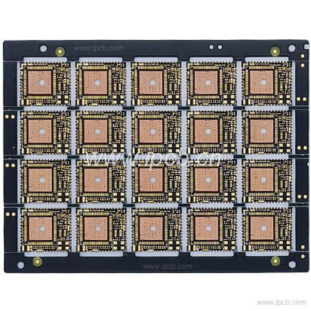
Ultra-high speed PCB gold finger board
Because the high-frequency current is generated by the ground noise voltage and the voltage drop in the wiring area of the digital device, multi-point grounding should be preferred in the design of high-speed digital PCBs. Its main purpose is to establish a unified potential common mode reference system. Because the parasitic parameters change the expected grounding path, single-point grounding cannot work effectively. As long as a low ground reference impedance is maintained, the ground loop usually has no digital problems.
Many digital loops do not require a grounded reference source with filtering. Digital circuits have a noise tolerance of several hundred millivolts and can withstand ground noise gradients of tens to hundreds of millivolts. The ground "mirror" plane in a multi-layer PCB circuit board is most suitable for signal currents. In order to control the loss caused by common mode return, the chassis should be grounded at multiple points.