PCB design basic knowledge
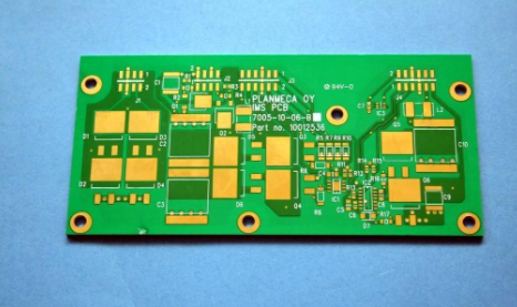
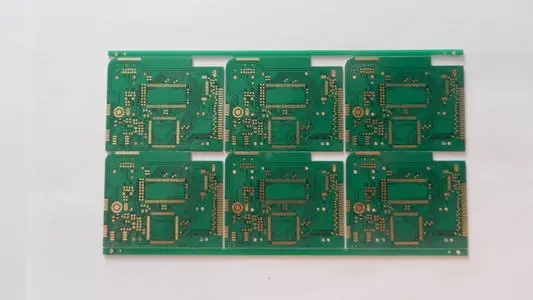
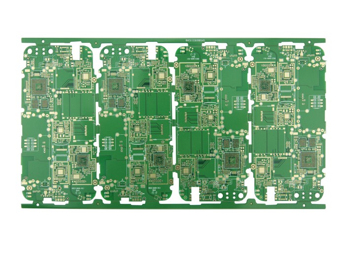
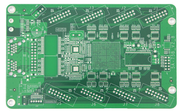
Printed circuit boards (PCBS) are found in almost every kind of electronic device. If there are electronic components in a piece of equipment, they are also embedded in various sizes of PCB. In addition to fixing various small parts, the main function of the PCB is to provide electrical connections between the components. As electronic equipment becomes more and more complex, more and more parts are needed, and the wiring and parts on the PCB become more and more dense. A standard PCB looks something like this. Bare Board(without parts on it) is also often referred to as "Printed Wiring Board(PWB)".

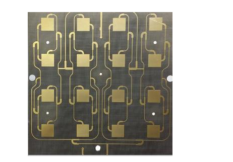
The substrate of the board itself is made of a material that is insulated and resistant to bending. The small line material that can be seen on the surface is copper foil. Originally, the copper foil is covered on the whole board, and the middle part is etched away in the manufacturing process, and the remaining part becomes a network of small lines. These lines are called conductors or conductors and are used to provide electrical connections to parts on the PCB.
To secure parts to the PCB, we solder their pins directly to the wiring. On a basic PCB, the parts are concentrated on one side and the wires are concentrated on the other. So we need to make holes in the board so that the pins can go through the board to the other side, so the pins of the parts are welded to the other side. Because of this, the front and back sides of a PCB are called Component Side and Solder Side respectively.
If there are parts on the PCB that can be removed or put back on after manufacture, Socket will be used to install the parts. Because the socket is directly welded to the board, the parts can be arbitrarily disassembled. A ZIF(Zero Insertion Force) plug allows parts to be inserted and removed easily.The lever next to the socket can hold the parts in place after you insert them.
To connect two PCBS to each other, an edge connector is commonly used. The gold finger contains a number of bare copper pads that are actually part of the PCB wiring. Normally, to connect, we insert the gold finger on one PCB into the appropriate Slot (commonly called expansion Slot) on the other PCB. In computers, display cards, sound cards, and similar interface cards are connected to the motherboard by means of a gold finger.
The green or brown color on the PCB is the color of the solder mask. This layer is an insulating shield that protects the copper wire and prevents parts from being welded to the wrong place. Another silk screen will be printed on the solder resistance layer. It is usually printed with words and symbols (mostly white) to indicate the position of the parts on the board. Screen printing is also known as legend.
Single-sided Boards
As we mentioned, on a basic PCB, the parts are concentrated on one side and the wires are concentrated on the other. Because the wire appears on only one side, we call this TYPE of PCB single-sided. Because single panels had many strict restrictions on the design of the circuit (because there was only one side, the wiring could not cross and had to take a separate path), only early circuits used such boards.
Double-sided Boards
The circuit board has wiring on both sides. But in order to use both wires, there must be proper electrical connections between the two sides. This "bridge" between circuits is called a guide hole (VIA). Guide holes are small holes in the PCB board that are filled or coated with metal and can be connected to wires on both sides. Because a dual panel has twice the area of a single panel, and because the wiring can be interlaced (it can be wound around to the other side), it is better for more complex circuits than a single panel.