How to design a PCB suitable for high-tech applications
Since the second industrial revolution in the 19th century, human science and technology have advanced by leaps and bounds, especially after human beings entered the 21st century, new infrastructure, new energy, artificial intelligence and other high-tech fields have developed rapidly. The low-frequency, low-speed, low-density, and low-performance circuit boards such as single-panel and double-panel are gradually eliminated.
Therefore, the requirements of high-tech products on circuit boards are becoming more and more demanding. The application of high-level, high-speed, high-frequency, high-end, high-density, and high-difficulty PCB boards is becoming more and more extensive. This type of PCB circuit board is the future PCB. The development trend of the industry.
So, how can we design high-performance circuit boards used in these areas. We specially invited senior PCB designers from Shenzhen Benqiang Circuit Co., Ltd. to share their design experience with you.
1.1 Signal integrity design
As an excellent PCB designer, you must consider the signal integrity (SI), electromagnetic interference (EMI) and impedance requirements of the circuit board. These factors are involved in the structure of the multilayer PCB: layer number, power supply and grounding Number of layers, layer sequence, layer spacing, etc. It is hoped that the signal layer is adjacent to the power layer, and the high-speed signal traces should be located in the inner layer between the power layers to achieve the best shielding; the power layer and the ground layer should be as close as possible, reduce the thickness of the dielectric layer and use a higher dielectric constant (Dk) substrate to achieve the best parasitic capacitance distribution [1].
If the design is an impedance-controlled circuit board, the designer can specify slightly different trace widths for different target impedances, especially when differential impedance is involved. For example, in the fourth layer of a multilayer board, 125 μm (5 mil) width traces are required to obtain a target impedance of 50 ohms, while 125 μm width traces are used in the same layer to obtain a differential impedance of 100 ohms. Then, input 128 μm (5.1 mil) width for the former single-ended trace design, and input 122 μm (4.9 mil) width for the latter differential trace. In this way, the manufacturer can meet the two impedance targets independently without having to compromise on either [2].
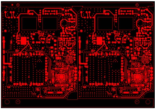
2nd order HDI board designed by Benqiang Company for automotive communication
The advantages of HDI boards include good high-frequency signal integrity and electrical performance. The improvement of signal integrity is due to the smaller substrate and shorter interconnection lines, smaller vias, and thinner dielectric layers, thereby reducing wiring Delay can improve signal integrity. For example, in order to overcome noise, radio frequency interference (RFI) and electromagnetic interference (EMI) for high-frequency and high-speed circuits on PCBs, using HDI board micro-via (aperture not greater than 0.15 mm) technology is currently one of the most feasible solutions.
The current high-performance PCB design process is equipped with an automatic design rule check (DRC) tool, which can be repeatedly checked during the design process and corrected in time, saving time, effort and accuracy. Automatic DRC includes layout DRC, electrical DRC, and electrical rule checking tools include signal integrity (SI), power integrity (PI), electromagnetic compatibility (EMC), anti-electromagnetic interference (EMI), and safety inspections.
1.2 Thermal management design
Heat dissipation is very important for the normal operation and long-term stability of electronic equipment. Therefore, there are thermal management requirements, that is, the management of heat or temperature of a system. From IC packaging to PCB and the entire electronic system, heat generation factors must be considered, and reasonable heat dissipation methods must be adopted.
Thermal issues should be considered at the beginning of PCB design. First, optimize the design to simplify thermal management methods and reduce costs. Optimal design factors affecting thermal performance, involving component location and PCB layout, should make the best use of system airflow for cooling; estimate the power of the main heating components, make thermal simulations, and try to select the same functional components with less heat generation; for high heat The component area determines whether a radiator is needed and selects a suitable radiator; select the PCB type and material to meet the heat dissipation conditions [3].
There are professional design, thermal simulation and thermal testing EDA tools on the market, innovatively using thermal barrier (Bn) and thermal shortcut (Sc) analysis techniques. Now engineers can use a non-destructive way (that is, without dividing the original sample to see the thermal characteristics inside), they can clarify where the heat flow of the IC, PCB, or the entire system is obstructed, and why the heat flow failure occurs, and at the same time Can determine the fastest and most effective heat dissipation shortcut to solve the heat dissipation design problem. [4] There is thermal risk management (TRM) simulation software, which can predict the temperature conditions of PCB circuits, including the temperature conditions of wires, through holes, surface media and layers.
PCB designers have many options to eliminate the heat generated by the components. At present, most of them are to directly attach a metal plate to the PCB to help dissipate heat, that is, a metal-based PCB or a metal-core PCB. The choice of thermal management solutions needs to balance a variety of factors. How to remove heat without increasing the size and weight of circuit boards and components. There are six typical heat dissipation methods: (1) Choose a suitable PCB substrate, from the standard Type to thermal conductivity type; (2) PCB conductor copper thickness develops to thick copper type; (3) Use PCB via holes to fill copper for heat conduction; (4) PCB external heat sink, that is, additional metal substrate; (5) PCB internal heat sink, That is, additional metal core board; (6) PCB is partially embedded with metal blocks. Designers can even combine other methods when choosing the next method [5].