In order to facilitate the production of PCB boards, PCB circuit board imposition generally must be designed with circuit board Mark points, V-shaped grooves, and processing edges. The senior engineers of Benqiang Circuit will consider the following points when designing to ensure the convenience of production and the high pass rate of the products.

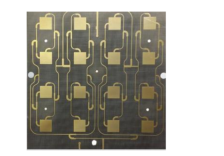
PCB puzzle
1. The appearance design of PCB jigsaw
1. The frame (clamping edge) of the PCB splicing method should adopt a closed-loop control design scheme to ensure that the PCB splicing method is fixed and not easy to deform after being installed on the fixture.
2. The total width of PCB splicing method is ≤260Mm (SIEMENS line) or ≤300mm (FUJI line); if automatic gluing is required, the total width of PCB splicing method is 125mm * 180mm.
3. The appearance design of the PCB boarding method is as close to the square as possible, and it is strongly recommended to use the 2*2, 3*3,...
PCB circuit board V-groove
2. PCB circuit board V-groove
1. After opening the V-groove, the remaining thickness X should be (1/4~1/3) the plate thickness L, but the minimum thickness X must be ≥0.4mm. Restrictions can be used for boards with heavy loads, and lower limits can be used for boards with lighter loads.
2. The displacement S of the wound on the left and right sides of the V-groove should be less than 0 mm; because of the minimum reasonable thickness limit, the V-groove splicing method is not suitable for the board with a thickness of less than 1.3mm.
3. Mark point
1. When setting the standard selection point, generally vacate an unobstructed non-resistance area 1.5 mm larger than the periphery of the selection point.
2. Used to assist the electronic optics of the SMT placement machine to accurately locate the top corner of the PCB circuit board with chip components. There are at least two different measuring points. The measuring point for the precise positioning of a whole PCB is generally one. The relative position of the top corner of the whole PCB; the measuring point for precise positioning of the electronic optics of the layered PCB is generally at the opposite position of the top corner of the layered PCB circuit board.
3. For components of QFP (square flat package) with wire spacing ≤0.5 mm and BGA (ball grid array package) with ball spacing ≤0.8 mm, in order to improve the precision of the chip, it is specified to set at the two top corners of the IC Measuring point.
Fourth, the processing technology side
1. Jigsaw method: The border between the border and the internal motherboard, the node between the motherboard and the motherboard cannot be large or overhanging components, and the edge of the electronic device and the PCB circuit board should leave more than 0.5 mm of indoor space. To ensure the normal operation of laser cutting CNC blades.
5. Precise positioning holes on the circuit board
1. It is used for the precise positioning of the entire board of the PCB circuit board and the standard mark for the precise positioning of fine-spaced components. Under normal circumstances, the QFP with an interval of less than 0.65mm should be set at the top corner of the board; The precise positioning standard marks of the PCB daughter board should be applied in pairs and laid out at the top corners of the precise positioning factors.
2. Precise positioning posts or precise positioning holes should be reserved for large electronic components, such as I/O jacks, microphones, rechargeable battery jacks, toggle switches, earphone jacks, motors, etc.
The above is an introduction to several places that engineers should pay attention to in PCB imposition. Ipcb is also provided to PCB manufacturers and PCB manufacturing technology.