Today's leading chip design needs to break through the new measurement categories of optical based target approximate calculation, statistical sampling, and single-layer control
PROVision ® 3E system provides engineers with millions of data points by integrating nano resolution, high-speed and penetration imaging, so as to meet their needs to correctly complete the graphics of the most advanced chip design
We have installed 30 sets of this system for the world's leading foundry logic chips, DRAM and NAND customers
October 18, 2021, Santa Clara, California - Applied Materials today released its unique electron beam measurement system. The system enables a new strategy for graphical control based on measurement on large-scale devices, cross wafer measurement and penetration measurement.
PROVision ® Based on the new graphical control strategy, 3E system provides engineers with millions of data points by integrating nano resolution, high-speed and penetration imaging, so as to meet their needs of correctly completing the graphical design of the most advanced chip
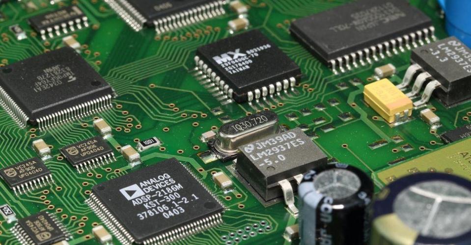
Advanced chips are built layer by layer. Billions of independent features must be perfectly mapped and aligned one by one in order to manufacture normal transistors and interconnection structures with photoelectric characteristics. With the transformation of the whole industry from simple two-dimensional design to more radical multi graphical and three-dimensional design, measurement methods also need corresponding breakthroughs to improve each key level in order to achieve the best performance, power, area cost and time to market (ppact) ™).
Traditional graphical control strategy
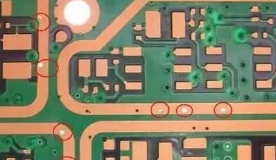
Traditionally, the graphic control is realized by using optical lithography measuring equipment to help keep the graphics on the grain consistent with the "lithography marks". These lithography marks are engraved between the grain and the grain through the mask, and will be removed from the wafer when slicing. The approximate value of the lithography marks can be calculated by sampling the data of the whole wafer.
However, after successive generations of feature miniaturization, the wider adoption of multiple graphics, and the introduction of 3D design leading to interlayer distortion, the measurement defects or "blind spots" caused by traditional methods are increasing, which makes it increasingly difficult for engineers to correctly associate the expected graphics with the on-chip results.
New graphical control strategy
With the birth of the new electron beam system technology, customers can directly and high-speed measure the semiconductor device structure across the whole wafer and across all levels, and customers can stride towards the transformation of a new graphical control strategy based on big data. Provision ® 3E system is the latest electron beam measurement innovation technology specially designed by applied materials company for this new strategy.
Keith wells, vice president of Applied Materials Group and general manager of imaging and process control division, said: "As a leader in electron beam technology, applied materials is providing customers with a new graphical control strategy, which is optimized for the most advanced logic chips and memory chips. The resolution and speed of provision 3E system enable it to break through the blind spot of optical measurement, not only across the whole wafer, but also between multiple different levels of the chip Accurate measurement provides chip manufacturers with cubes to meet their needs to improve PPAC and accelerate the rapid launch of new process technologies and chips. "
Provision 3E system
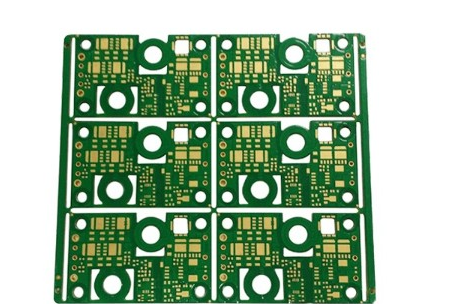
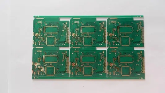
The provision 3E system contains a variety of technical features to support the graphical control capability required by the most advanced design, including 3-nm wafer foundry logic chip, full surround gate transistor, next-generation DRAM and 3D NAND.
Resolution: the industry-leading electron beam barrel technology of applied materials company can provide the highest electron density that can be achieved at present and support fine imaging with 1 nm resolution.
Accuracy: with decades of CD SEM system and algorithm expertise, provide accurate and high-precision measurement for key features.
Speed: it can perform 10 million measurements per hour, and the measurement results are accurate and feasible.
Multilayer: unique elluminator of Applied Materials ® The technology can capture 95% of the backscattered electrons to quickly measure the key dimensions and edge layout of multiple levels at the same time.
Range: support a wide range of electron beam energy levels. High energy mode supports rapid measurement with a depth of hundreds of nanometers. Low energy mode supports nondestructive measurement of various brittle materials and structures, including EUV photoresist
By combining these features, customers can get rid of the old graphical control strategy composed of optical imprint identification approximate calculation, limited statistical sampling and single-layer control, and realize a new strategy based on on on-chip, cross wafer and penetration measurement and control of large-scale devices.
Process menu optimization
Provision 3E system is also AIX (effective insight accelerator) of applied materials company Key components of the platform, which organically combines process technology, sensors and data analysis, so that each stage of process technology development, from R & D, capacity climbing to mass production, can be significantly accelerated without exception. AIX platform analysis associates process variables with the measurement results on wafers captured by provision 3E to help engineers speed up process development Double and expand the process window by 30%