In any switching power supply design, the physical design of the PCB board is the last link. If the design method is improper, the PCB may radiate too much electromagnetic interference, resulting in the unstable work of the power supply. The following is an analysis of the matters needed to pay attention to in each step.
1. Establish component parameters from schematic diagram to PCB design process -- > Input principle netlist - > Design parameter setting - > Manual layout - > Manual cabling - > Validate design -- > Review - & gt; CAM output.
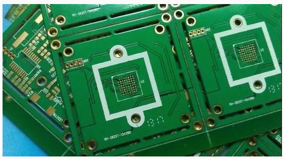
2. Parameter setting The spacing between adjacent wires must meet the requirements of electrical safety, and in order to facilitate operation and production, the spacing should be as wide as possible. The minimum spacing should be suitable for the voltage at least. When the wiring density is low, the spacing of signal lines can be appropriately increased. For the signal lines with high and low level disparity, the spacing should be as short as possible and the spacing should be increased. The distance between the edge of the inner hole of the pad and the edge of the printed board should be greater than 1mm to avoid defects of the pad during machining. When the wire connected with the pad is relatively thin, the connection between the pad and the wire is designed into a droplet shape. The advantage is that the pad is not easy to peel, but the wire and the pad is not easy to disconnect.

3. Component layout Practice has proved that even if the circuit schematic design is correct and the printed circuit board design is improper, the reliability of electronic equipment will be adversely affected. For example, if two thin parallel lines of a printed board are close together, there will be a delay in the signal waveform, resulting in reflected noise at the end of the transmission line. The interference caused by the power supply and grounding wire will degrade the performance of the product. Therefore, when designing the printed circuit board, attention should be paid to the correct method.Each switching power supply has four current loops: power supply switching AC loop output rectifier AC loop input signal source current loop output load current loop Input loop through an approximate DC current to charge the input capacitor, filter capacitor mainly plays a broadband energy storage role; Similarly, output filter capacitors are used to store high frequency energy from the output rectifier while eliminating dc energy from the output load loop. Therefore, the wiring terminals of the input and output filter capacitors are very important. The input and output current loops should be connected to the power supply only from the wiring terminals of the filter capacitor respectively. If the connection between the input/output circuit and the power switch/rectifier circuit cannot be directly connected to the capacitor's terminal, ac energy will pass through the input or output filter capacitor and radiate into the environment. The ac circuits of the power supply switch and the rectifier contain high-amplitude trapezoidal currents, which have a high harmonic component and a frequency much higher than the fundamental frequency of the switch. The peak amplitude can be up to 5 times that of the continuous input/output dc current. The transition time is usually about 50ns. The two circuits are most likely to produce electromagnetic interference, so must the other printed wiring in power source to cloth before these ac circuits, each loop three main components of the filter capacitor, the power switch or rectifier, inductor or transformer shall be placed adjacent to each other, adjust the current path between the element position make them as short as possible.
4. Control circuit design connected to the AC power circuit Input current source loop and input filter Design Output load loop and output filter According to the functional unit of the circuit, the layout of all components of the circuit should comply with the following principles:
Consider the PCB size first. When the PCB size is too large, the printed line is long, the impedance increases, the anti-noise ability decreases, and the cost increases. Too small heat dissipation is not good, and adjacent lines are susceptible to interference. The best shape of the circuit board is rectangular, length to width ratio 3:2 or 4:3, components located on the edge of the circuit board, generally not less than 2mm from the edge of the circuit board. Place the components to consider future welding, not too dense. Center on the core components of each functional circuit, and layout around it. Components should be evenly, neatly and compact arranged on the PCB, minimizing and shortening the leads and connections between components, and decoupling capacitance as close as possible to the VCC of the device. For circuits working at high frequencies, distribution parameters between components should be considered. In general circuits, components should be arranged in parallel as much as possible. In this way, not only beautiful, but also easy to install and weld, easy to mass production. According to the circuit process arrangement of each functional circuit unit position, so that the layout is easy to signal circulation, and make the signal as far as possible to maintain the same direction. The first principle of layout is to ensure the wiring of the distribution rate, mobile devices pay attention to the connection of flying lines. Reduce the loop area as much as possible to suppress the radiation interference from the switching power supply.
5. Wiring switch power supply contains high frequency signal, any printed line on PCB can play the role of antenna, the length and width of printed line will affect its impedance and inductive reactance, thus affecting the frequency response. Even printed lines that pass through dc signals can be coupled to rf signals from adjacent printed lines and cause circuit problems (or even re-radiate interference signals). All printed lines running through ac current should therefore be designed to be as short and wide as possible, which means that all components connected to printed lines and to other power lines must be placed close together.
The length of the printed line is directly proportional to its inductance and impedance, and the width is inversely proportional to the inductance and impedance of the printed line. The length reflects the wavelength of the printed line's response. The longer the length, the lower the frequency of the printed line can send and receive electromagnetic waves, and the more rf energy it can radiate. According to the size of the printed circuit board current, as far as possible to increase the width of the power line, reduce the resistance of the loop. At the same time, make the power line, ground line and current direction consistent, which helps enhance the anti-noise ability. Grounding is the bottom branch of four current circuits of switching power supply, which plays a very important role as the common reference point of the circuit, and it is an important method to control interference. Therefore, carefully consider the grounding cables in the layout. Mixing grounding cables may cause unstable power supply.
6. Check the wiring design is completed, it is necessary to carefully check the wiring design by the designers is in line with the rules, rules at the same time also need to confirm whether accord with the demand of the PCB production process, general inspection line to line, line and element bonding pad, the line and communicating pores, element bonding pad and communicating pores, through hole and the distance between the through hole is reasonable, whether to meet the production requirements. Whether the width of the power cord and ground wire is appropriate, and whether there is room for the ground wire to be widened in the PCB. Note: Some errors can be ignored, for example, part of Outline of some connectors is placed outside the board frame, so it will be wrong to check the spacing; In addition, after each modification of the wiring and hole, it is necessary to re-coat copper once. Review according to the "PCB checklist", including design rules, layer definition, line width, spacing, pads, hole Settings, but also focus on the review of the rationality of device layout, power supply, grounding network wiring, high-speed clock network wiring and shielding, decoupling capacitor placement and connection.