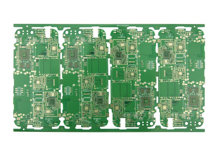
How is a PCB born? PCB manufacturers take you through
I want to show you how a PCB board was born. First of all, how was the PCB born? Before the appearance of the PCB, the circuit was composed of point-to-point wiring. This way...
How did the Honglian Circuit PCB come into being today? Before the appearance of the PCB, the circuit was composed of point-to-point wiring. The reliability of this method is very low, because as the circuit ages, the rupture of the circuit will cause the circuit node to open or short circuit. Winding technology is a major advancement in circuit technology. This method improves the durability and replaceability of the circuit by winding small-diameter wires on the poles at the connection point. As the electronics industry develops from vacuum tubes and relays to silicon semiconductors and integrated circuits, the size and price of electronic components are also falling. Electronic products appear more and more frequently in the consumer field, prompting manufacturers to find smaller and more cost-effective solutions. Thus, the PCB was born.
The first step in PCB production is to organize and check the PCB layout. The PCB production factory receives the CAD files from the PCB design company. Since each CAD software has its own unique file format, the PCB factory will convert it into a unified format-Extended Gerber RS-274X or Gerber X2. Then the factory's engineers will check whether the PCB layout conforms to the manufacturing process and whether there are any defects and other issues.
Clean the copper clad laminate, if there is dust, it may cause the final circuit to be short-circuited or broken.
It is made up of 3 copper clad laminates (core boards) plus 2 copper films, and then glued together with prepregs. The production sequence is to start from the middle core board (4 and 5 layers of lines), continuously stack together, and then fix. The production of 4-layer PCB is similar, except that only one core board and two copper films are used.
To transfer the inner PCB layout, first make the two-layer circuit of the middle core board(Core). After the copper clad laminate is cleaned, it will be covered with a photosensitive film on the surface. This film will solidify when exposed to light, forming a protective film on the copper foil of the copper clad laminate.
Insert the two-layer PCB layout film and the double-layer copper clad laminate, and finally insert the upper PCB layout film to ensure that the upper and lower PCB layout films are stacked accurately.
The light machine irradiates the photosensitive film on the copper foil with a UV lamp. The photosensitive film is cured under the transparent film, and there is still no cured photosensitive film under the opaque film. The copper foil covered under the cured photosensitive film is the required PCB layout circuit, which is equivalent to the function of the laser printer ink of the manual PCB.

Then use lye to clean the uncured photosensitive film, and the required copper foil circuit will be covered by the cured photosensitive film.
Then use a strong base, such as NaOH, to etch away the unnecessary copper foil.
Tear off the cured photosensitive film to expose the copper foil of the required PCB layout.
The core board has been successfully produced. Then punch alignment holes on the core board to facilitate alignment with other materials. Once the core board is pressed together with other layers of PCB, it cannot be modified, so inspection is very important. The machine will automatically compare with the PCB layout drawing to check for errors.
A new raw material is needed here, called a prepreg, which is the adhesive between the core board and the core board (PCB layers>4), as well as the core board and the outer copper foil, and it also plays a role in insulation.
The lower copper foil and the two layers of prepreg have been fixed in advance through the alignment hole and the lower iron plate, and then the finished core board is also placed in the alignment hole, and finally the two layers of prepreg, a layer of copper foil and A layer of pressure-bearing aluminum plate covers the core plate.
The PCB boards clamped by the iron plates are placed on the support, and then sent to the vacuum heat press for laminating. The high temperature in the vacuum hot press can melt the epoxy resin in the prepreg and fix the core boards and copper foils together under pressure.
After the lamination is completed, remove the upper iron plate that presses the PCB. Then remove the pressure-bearing aluminum plate. The aluminum plate also has the responsibility of isolating different PCBs and ensuring the smoothness of the outer copper foil of the PCB. Both sides of the PCB taken out at this time will be covered by a layer of smooth copper foil.
To connect 4 layers of non-contact copper foils in the PCB, first drill through the through holes to open the PCB, and then metalize the hole walls to conduct electricity.
Use the X-ray drilling machine to locate the inner core board. The machine will automatically find and locate the hole on the core board, and then punch the positioning hole on the PCB to ensure that the next hole is drilled from the center of the hole. Over.
Put a layer of aluminum plate on the punching machine machine, and then put the PCB on it. In order to improve efficiency, according to the number of PCB layers, 1 to 3 identical PCB boards are stacked together for perforation. Finally, cover the uppermost PCB with a layer of aluminum plate. The upper and lower layers of aluminum plate are used to prevent the copper foil on the PCB from tearing when the drill bit drills in and out.
In the previous lamination process, the molten epoxy was squeezed out of the PCB, so it needed to be cut off. The profiling milling machine cuts its periphery according to the correct XY coordinates of the PCB.
Since almost all PCB designs use perforations to connect different layers of lines, a good connection requires a 25-micron copper film on the hole wall. The thickness of the copper film needs to be achieved by electroplating, but the hole wall is composed of non-conductive epoxy resin and glass fiber board.
So the first step is to deposit a layer of conductive material on the hole wall, and form a 1 micron copper film on the entire PCB surface by chemical deposition, including the hole wall. The entire process such as chemical treatment and cleaning is controlled by the machine.
Next, the PCB layout of the outer layer will be transferred to the copper foil. The process is similar to the previous inner core PCB layout transfer principle, which is to transfer the PCB layout to the copper by using photocopying film and photosensitive film. On the foil, the only difference is that the positive film will be used as the board.
The internal PCB layout transfer uses the subtractive method, and the negative film is used as the board. The PCB is covered by the cured photosensitive film as a circuit, and the uncured photosensitive film is cleaned. After the exposed copper foil is etched, the PCB layout circuit is protected by the cured photosensitive film.
The transfer of the outer PCB layout adopts the normal method, and the positive film is used as the board. The non-circuit area is covered by the cured photosensitive film on the PCB. After cleaning the uncured photosensitive film, electroplating is performed. Where there is a film, it cannot be electroplated, and where there is no film, copper is plated first and then tin is plated. After the film is removed, alkaline etching is performed, and finally the tin is removed. The circuit pattern remains on the board because it is protected by tin.
Clamp the PCB with clamps, and electroplate the copper. As mentioned earlier, in order to ensure that the holes have sufficient conductivity, the copper film plated on the hole walls must have a thickness of 25 microns, so the entire system will be automatically controlled by the computer to ensure its accuracy.
Next, a complete automated assembly line completes the etching process. First, clean the cured photosensitive film on the PCB. Then use a strong alkali to clean the unnecessary copper foil covered by it. Then use the tin stripping solution to strip the tin plating on the PCB layout copper foil. After cleaning, the 4-layer PCB layout is complete.