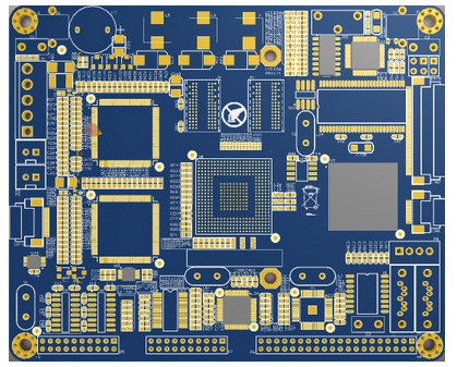
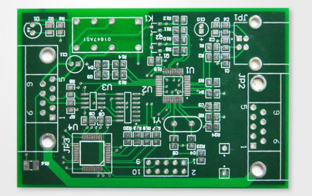
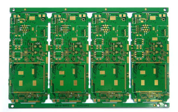
Introduction of HDI circuit board
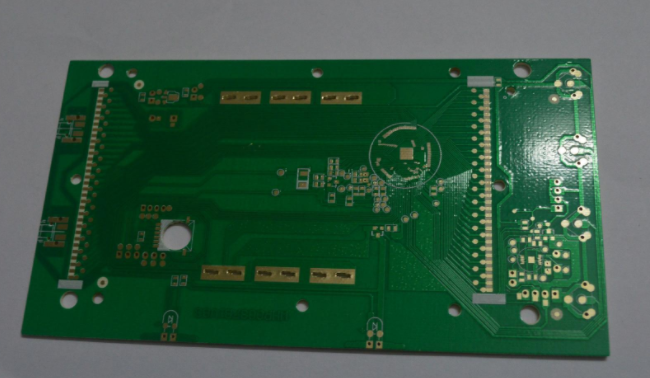
HDI board (English is high-densityinterconnectboard) is a kind of circuit board with high wiring density in micro-blind via technology. The HDI board is divided into an inner layer circuit and an outer layer circuit, and the internal connection of each layer circuit board is realized through the method of drilling and metallization.
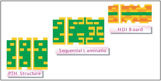
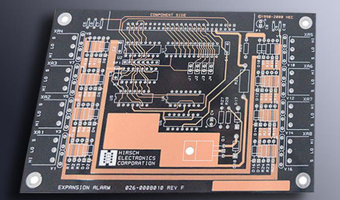
Therefore, the higher the application of HDI technology, the higher the level of laminate manufacturing. The ordinary HDI board is laminated once, and the high-end HDI adopts two, three or more lamination processes, as well as electroplating to fill holes, pile holes, and laser direct drilling.
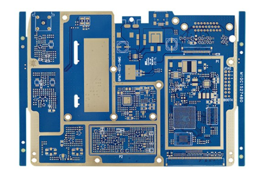
Are all blind and buried PCB circuit boards called HDI circuit boards?
The HDI board is a high-density interconnect circuit board. After the blind hole is plated, the floor is HDI board after pressing twice. HDi boards are divided into 1, 2, 3, 4 and 5 HDI boards. For example, for mobile phones after iphone6, the motherboard uses 5th order HDI. So simply buried via is not necessarily an hdi circuit board.

How to identify the 1st, 2nd and 3rd order of the hdi circuit board
The easiest thing for everyone to understand is: Level 1 is the easiest to produce, and it is relatively easy to control in terms of parameters and technology. Tier 2 and above are relatively difficult, especially Tier 5 is the most difficult to control.