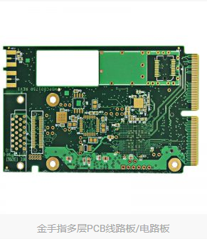
The difference between PCB multi-layer circuit board V cut and stamp hole
There are several definitions of PCB multilayer circuit board Ask to do it. The convenience of PCB multilayer circuit board manufacturers to produce is to facilitate V-cutting and so on. The purpose of saving materials is to use materials more perfectly without wasting or leaving too much side material! For example, for materials of 1 meter 2 by 1 meter, you will be perfect when you open a 34X41CM jigsaw.
In order to join the board, it is necessary to consider the connection methods between the PCB multi-layer circuit boards. Generally, there are three kinds: V-cut (V-CUT), stamp hole and hollow connection strip. V-cut is used more for regular boards, as long as the two PCB multi-layer circuit boards are put together, leaving a gap (V-cut gap) between them. Stamp holes are often used in special-shaped boards, and multiple vias are placed at the connection of the PCB multi-layer circuit board. Hollow connecting strips use very narrow plates for connection, which are more commonly used in boards with half-hole technology.
Is the V cut of the PCB multi-layer circuit board or the stamp hole better?
1. V cut
V-cut, also known as V-CUT, is to draw a slot at the junction of two PCB multi-layer circuit boards, where the connection of the boards is relatively thin and easy to break. It is enough to merge the edges of the two PCB multi-layer circuit boards together when joining the board. In addition, V-cuts are generally straight lines, and there are no complicated traces such as curved arcs, so you can try to be in a straight line when making up. Note that there is a gap between the two PCB multi-layer circuit boards for the V cut, generally 0.4mm is sufficient. The V secant can be represented by using 2D lines on all layers.

Since the V-cut can only go straight, it is only suitable for the connection of regular PCB multi-layer circuit boards. For irregular PCB multilayer circuit boards, such as round ones, stamp holes are needed to connect the boards. Below, Shenzhen Zhongke Circuit introduces the stamp holes.
2. Stamp hole
Stamp hole is another connection method of PCB multi-layer circuit board jigsaw, which is generally used more in special-shaped boards. The edges of the two PCB multi-layer circuit boards are connected by a small plate, and the connection between this small plate and the two PCB multi-layer circuit boards has many small holes, so it is easy to break.
It is called a stamp hole because the edge of the board is like the edge of a stamp after the break.
3. Hollow connecting strip
The connection method is similar to the stamp hole, the difference is that the connecting part of the connecting strip is a bit narrower, and there are no vias on both sides. One disadvantage of this method is that after the PCB multi-layer circuit board is broken, there will be a very obvious bump, and the bump of the stamp hole is not so obvious because it is separated by the via hole. In this case, why use this method? Just use the stamp hole directly. In fact, there is a situation where neither the stamp hole nor the V-cut can be used, that is, when the module is made with a half hole on all sides, it can only be connected at the four corners of the module by hollow connecting strips.