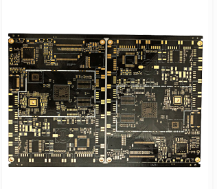
Blind and buried via circuit board: high-precision circuit board explanation
With the development of electronic products towards high density and high precision, the same requirements have been put forward on PCB circuit boards. The most effective way to increase the density of blind buried vias is to reduce the number of vias, and accurately set blind and buried vias to meet this requirement, thus forming HDI blind buried vias.
HDI blind buried via circuit board is a compact product designed for small-capacity users. It adopts modular and parallel design. A module has a capacity of 1000VA (1U height) and has been naturally cooled. It can be placed directly in a 19-inch rack, and up to 6 modules can be connected in parallel. The product adopts all-digital signal process control (DSP) technology and a number of patented technologies. Regardless of the load power factor and crest factor, it has a comprehensive adaptive load capacity and a strong short-term overload capacity.

HDI blind buried vias are mainly manufactured using blind micro vias and buried via technology. It is characterized in that the electronic circuits in the printed circuit board can be distributed with a higher circuit density, and due to the substantial increase in circuit density, the printed circuit board made of HDI blind buried vias cannot be used. Generally, for drilling, HDI must use a non-mechanical drilling process. There are many non-mechanical drilling methods. Among them, "laser drilling" is the main hole-forming solution for HDI circuit board high-density interconnection technology.
HDI blind buried vias circuit boards are usually manufactured by stacking methods. The longer the build time, the higher the technical level of the circuit board. It can reduce the cost of blind buried vias (PCB high multi-layer circuit boards): when the density of PCB increases to more than eight layers, it is manufactured with HDI blind buried vias, and its cost will be lower than the traditional complex Suppressing process.