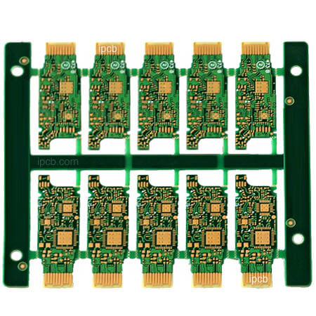
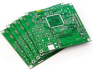
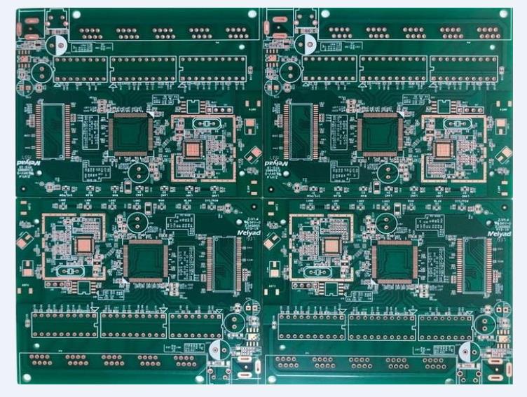
PCB, also known as Printed Circuit Boards, can realize circuit connection and function realization between electronic components, and is also an important part of power circuit design. Today, this article will introduce the basic rules of PCB layout and wiring.

1. Basic Rules of Component Layout
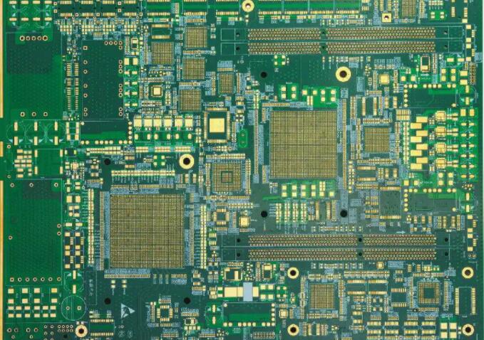
1. Layout according to the circuit module, the related circuits that realize the same function are called a module, the components in the circuit module should adopt the principle of nearby concentration, and the digital circuit and the analog circuit should be separated;
2. Do not mount components and devices within 1.27mm around non-mounting holes such as positioning holes and standard holes, and do not mount components within 3.5mm (for M2.5) and 4mm (for M3) around mounting holes such as screws;
3. Avoid placing vias below components such as horizontally mounted resistors, inductors (plug-ins), and electrolytic capacitors to avoid short circuits between the vias and the component shell after wave soldering;
4. The distance between the outside of the component and the edge of the board is 5mm;
5. The distance between the outside of the pad of the mounted component and the outside of the adjacent component is greater than 2mm;
6. Metal shell components and metal parts (shielding boxes, etc.) cannot touch other components, and cannot be close to printed lines and pads, and the spacing should be greater than 2mm. The size of the positioning holes, fastener installation holes, elliptical holes and other square holes in the plate is greater than 3mm from the edge of the plate;
7. The heating element cannot be close to the wire and the thermal element; the high-heating element should be evenly distributed;
8. The power socket should be arranged around the printed board as much as possible, and the bus bar terminals connected to the power socket should be arranged on the same side. Special care should be taken not to arrange power sockets and other soldered connectors between the connectors, in order to facilitate the soldering of these sockets and connectors, and the design and tying of power cables. The arrangement spacing of power sockets and welding connectors should be considered to facilitate the insertion and removal of power plugs;
9. Arrangement of other components: All IC components are aligned on one side, polar components are marked clearly, and the polarity marking on the same printed board should not be more than two directions. When two directions appear, the two directions are perpendicular to each other. ;
10. The wiring on the board should be properly dense. When the difference in density is too large, it should be filled with mesh copper foil, and the mesh should be greater than 8mil (or 0.2mm);
11. There should be no through-holes on the patch pads, so as to avoid the loss of solder paste and cause the components to be soldered. Important signal lines are not allowed to pass between the socket pins;
12. The patch is unilaterally aligned, the character direction is the same, and the packaging direction is the same;
13. For devices with polarity, the direction of polarity marking on the same board should be as consistent as possible.
2. Component wiring rules
In the area where the wiring area is ≤1mm from the edge of the PCB, and within 1mm around the mounting hole, wiring is prohibited; 2. The power line should be as wide as possible and should not be less than 18mil; the signal line width should not be less than 12mil; cpu The incoming and outgoing lines should not be less than 10mil (or 8mil); the line spacing should not be less than 10mil; 3, the normal via hole should not be less than 30mil; 4, the dual in-line: pad 60mil, aperture 40mil; 55mil (0805 surface mount); 62mil pad, 42mil aperture when plugged directly; electrodeless capacitor: 51*55mil (0805 surface mount); 50mil pad, 28mil aperture when plugged directly; 5. Note that the power cord and ground wire should be as far as possible Radial, and the signal line cannot have loopback.
2.1 The following systems should pay special attention to anti-electromagnetic interference:
(1) The microcontroller clock frequency is particularly high, and the bus cycle is particularly fast.
(2) The system contains high-power, high-current drive circuits, such as spark-generating relays, high-current switches, etc.
(3) A system with a weak analog signal circuit and a high-precision A/D conversion circuit.
2.2 To increase the anti-electromagnetic interference capability of the system, take the following measures:
(1) Select a microcontroller with low frequency: Selecting a microcontroller with low external clock frequency can effectively reduce noise and improve the anti-interference ability of the system. Square waves and sine waves of the same frequency, the high frequency components in the square wave are much more than the sine wave. Although the amplitude of the high-frequency component of the square wave is smaller than that of the fundamental wave, the higher the frequency, the easier it is to emit and become a noise source. The influential high-frequency noise generated by the microcontroller is about 3 times the clock frequency.
(2) Reduce the distortion in signal transmission The microcontroller is mainly manufactured with high-speed CMOS technology. The static input current of the signal input terminal is about 1mA, the input capacitance is about 10PF, the input impedance is quite high, and the output terminal of the high-speed CMOS circuit has a considerable load capacity, that is, a considerable output value. The reflection problem is very serious when the long line is led to the input end with a relatively high input impedance, which will cause signal distortion and increase the system noise. When Tpd>Tr, it becomes a transmission line problem, and problems such as signal reflection and impedance matching must be considered. The delay time of the signal on the printed circuit board is related to the characteristic impedance of the lead, that is, related to the dielectric constant of the printed circuit board material. It can be roughly considered that the transmission speed of the signal on the printed board leads is about 1/3 to 1/2 of the speed of light. The Tr (standard delay time) of commonly used logic telephone elements in systems composed of microcontrollers is between 3 and 18 ns. On the printed circuit board, the signal passes through a 7W resistor and a 25cm long lead, and the on-line delay time is roughly between 4 and 20ns. That is to say, the shorter the signal leads on the printed circuit, the better, and the length should not exceed 25cm. And the number of vias should be as small as possible, no more than 2. When the rise time of the signal is faster than the delay time of the signal, it is processed according to fast electronics. At this time, the impedance matching of the transmission line should be considered. For the signal transmission between the integrated blocks on a printed circuit board, it is necessary to avoid the situation of Td>Trd. The larger the printed circuit board, the less the speed of the system can be too fast. A rule of thumb for printed circuit board design is summarized by the following conclusions: The delay time of the signal transmission on the printed circuit board should not be greater than the nominal delay time of the device used.
(3) Reduce the interference between signal lines:
A step signal with a rise time of Tr at point A is transmitted to terminal B through lead AB. The delay time of the signal on the AB line is Td. At point D, due to the forward transmission of the signal at point A, the reflection of the signal after reaching point B and the delay of the AB line, a page pulse signal with a width of Tr will be induced after Td time. At point C, due to the transmission and reflection of the signal on AB, a positive pulse signal with a width of twice the delay time of the signal on the AB line, that is, 2Td, will be induced. This is the cross-interference between signals. The strength of the interfering signal is related to the di/at of the signal at point C, and is related to the distance between lines. When the two signal lines are not very long, what is actually seen on AB is the superposition of two pulses. Microcontrollers manufactured by CMOS process have high input impedance, high noise, and high noise tolerance. The digital circuit is superimposed with 100~200mv noise and does not affect its work. If the AB line in the figure is an analog signal, this kind of interference becomes intolerable. For example, if the printed circuit board is a four-layer board, one of which is a large-area ground, or a double-sided board, when the reverse side of the signal line is a large-area ground, the cross-interference between such signals will become smaller. The reason is that the large area of ground reduces the characteristic impedance of the signal line, and the reflection of the signal at the D terminal is greatly reduced. The characteristic impedance is inversely proportional to the square of the dielectric constant of the medium between the signal line and the ground, and is proportional to the natural logarithm of the thickness of the medium. If the AB line is an analog signal, to avoid the interference of the digital circuit signal line CD to AB, there should be a large area of ground below the AB line, and the distance from the AB line to the CD line should be greater than 2~3 times the distance between the AB line and the ground. Partial shielding can be used, and ground wires are arranged on the left and right sides of the lead on the side with the lead junction.
(4) Reduce the noise from the power supply While supplying energy to the system, the power supply also adds its noise to the supplied power supply. The reset line, interrupt line, and other control lines of the microcontroller in the circuit are easily disturbed by external noise. Strong disturbances on the grid enter the circuit through the power supply, and even in battery-powered systems, the battery itself has high-frequency noise. Analog signals in analog circuits are more resistant to interference from power sources.
(5) Pay attention to the high-frequency characteristics of printed circuit boards and components. In the case of high frequency, the leads, vias, resistors, capacitors, and distributed inductance and capacitance of connectors on the printed circuit board cannot be ignored. The distributed inductance of the capacitor cannot be ignored, and the distributed capacitance of the inductor cannot be ignored. The resistance will reflect the high-frequency signal, and the distributed capacitance of the lead will work. When the length is greater than 1/20 of the corresponding wavelength of the noise frequency, an antenna effect will occur, and the noise will be emitted through the lead. The vias of the printed circuit board cause a capacitance of about 0.6pf. The packaging material of an integrated circuit itself introduces 2~6pf capacitance. A connector on a circuit board has a distributed inductance of 520nH. A double row straight 24-pin integrated circuit holder, which introduces a distributed inductance of 4~18nH. These small distribution parameters are negligible for this line of microcontroller systems at lower frequencies; special attention must be paid to high-speed systems.
(6) The arrangement of components should be reasonably partitioned. The position of the components arranged on the printed circuit board should be fully considered against electromagnetic interference. One of the principles is that the leads between the components should be as short as possible. In the layout, the analog signal part, the high-speed digital circuit part, and the noise source part (such as relays, high-current switches, etc.) should be reasonably separated, so that the signals between them are coupled to each other. Handle the ground wire on the printed circuit board, the power wire and the ground wire are important. To overcome electromagnetic interference, the main means is grounding. For the double-sided panel, the ground wire layout is very particular. By adopting the single-point grounding method, the power supply and the ground are connected to the printed circuit board from both ends of the power supply, with one contact for the power supply and one contact for the ground. On the printed circuit board, there must be multiple return ground wires, and these will be gathered on the contact of the return power supply, which is the so-called single-point grounding. The so-called separation of analog ground, digital ground, and high-power device ground means that the wiring is separated, and all of them are brought together to this grounding point. When connecting to signals other than the printed circuit board, shielded cables are usually used. For high frequency and digital signals, the shielded cable is grounded at both ends. Shielded cables for low-frequency analog signals should be grounded at one end. Circuits that are very sensitive to noise and interference or circuits that are particularly high-frequency PCB board noise should be shielded with a metal cover.