1. Introduction to the production method of PCB board
1.1 Method 1:
(1) Cut the copper clad board to the size required for the circuit diagram.
(2) Put the wax paper on the steel plate, use a pen to engrave the circuit diagram on the wax paper at a ratio of 1:1, and cut the circuit diagram engraved on the wax paper according to the size of the circuit board, and place the cut wax paper on the printed copper plate. Take a small amount of paint and talc powder to make a suitable thin and thick printing material, dip the printing material with a brush, apply it evenly on the wax paper, repeat it several times, and the circuit can be printed on the printed board. This stereotype is reusable and suitable for small batches.
(3) Prepare a corrosion solution with 1 gram of potassium chlorate and 40 ml of hydrochloric acid with a concentration of 15%, and apply it to the place to be corroded on the circuit board for corrosion.
(4) Wash the corroded printed board with water repeatedly. Wipe off the paint with banana water and wash it a few more times to keep the printed board clean without leaving any corrosive liquid. Apply a layer of rosin solution to dry and drill holes.

1.2 Method 2:
(1) Drawing of the printing plate. The pads in the figure are represented by dots, and the connection can be a single line, but the location. The size needs to be accurate.
(2) Cut the printing plate according to the size of the printing plate, and clean the copper foil surface.
(3) Use carbon paper to copy the diagram to the printing board. If the circuit is relatively simple, and the maker has certain experience in making boards, this step can be omitted.
(4) According to the specific conditions of the actual components, paste standard pre-cut symbols (pads) with different inner and outer diameters; then, depending on the current, paste tape lines of different widths. 1.50) and so on, buy the paper-based material (black), and try not to use the plastic-based (red) material. The commonly used specifications of tape are 0.3.0.9.1.8. 2.3. 3.7 and so on. All units are millimeters.
(5) Use a softer hammer, such as smooth rubber. Tap the sticker with plastic, etc. to make it fully adhere to the copper foil. Focus on the corners of the line. lap joint. In cold weather, use a heater to warm the surface to enhance the adhesion.
(6) Put it into ferric chloride to corrode, but it should be noted that the liquid temperature is not higher than 40 degrees. After the corrosion, it should be taken out and rinsed in time, especially if there are thin lines.
(7) Punch holes, brighten the copper foil with fine sandpaper, apply rosin alcohol solution, and dry it to complete the production. The quality of this printed board is very close to the regular printed board. The 0.3mm tape can be passed between the two feet of the IC, which can greatly reduce the short jumpers on the front of the board to save trouble. save time.
1.3 Method 3:
Dissolve one part of the lacquer sheet (ie shellac, available in chemical raw material stores) in three parts of anhydrous alcohol, and stir it properly. Showing a certain color, after stirring evenly, it can be used as a protective paint to paint the circuit board. First polish the copper-clad plate with fine sandpaper, and then use the duckbill pen in the drawing instrument (or the ink duckbill pen used to draw graphics on the compass) to draw the drawing. The duckbill pen has a nut for adjusting the thickness of the stroke. Adjustable and can borrow a ruler. The triangle ruler draws very thin straight lines, and the drawn lines are smooth. Even, no jagged edges, giving a smooth finish. Fluent feeling; at the same time, you can also write Chinese characters in the free space of the circuit board. English. pinyin or symbol
If the drawn lines infiltrate into the surroundings, the concentration is too small, you can add a little varnish; if you can't drag the pen, it is too thick, and you need to add a few drops of anhydrous alcohol. It doesn't matter if the drawing is wrong, just use a small stick (matchstick), make a small cotton swab, dip it in a little anhydrous alcohol, you can easily wipe it off, and then redraw it. Once the circuit board is drawn, it can be etched in a ferric chloride solution. After the circuit board is corroded, it is also very convenient to remove the paint. With a cotton ball dipped in anhydrous alcohol, the protective paint can be wiped off. Due to the fast evaporation of alcohol, the prepared protective paint should be stored in a small bottle (such as an ink bottle) sealed and stored. Don't forget to close the bottle cap after use. If the concentration is thickened next time, just add an appropriate amount Anhydrous alcohol will do.
1.4 Method 4:
Paste the instant sticker on the copper foil of the copper-clad plate, then draw a circuit on the veneer, and then use a carving knife to carve through the veneer layer to form the required circuit, remove the non-circuit part and use ferric chloride to corrode or current electrolysis. The method can make a more ideal circuit board. The corrosion temperature can be carried out at about 55 degree Celsius, and the corrosion rate is faster. Rinse the corroded circuit board with clean water, remove the sticky notes on the circuit, make holes, wipe it clean and apply rosin alcohol solution for use.
1.5 Method 5:
(1) According to the shape of the components used in the circuit schematic diagram and the size of the printed board area, the density of the components and the position of each component should be reasonably arranged, and the rivet standoffs as fasteners should also be arranged reasonably. The location of the components should be determined according to the principle of the big first, the filial piety first, the whole and then the part, so that the adjacent components in the circuit are placed nearby and arranged neatly and evenly.
(2) The connecting wires between the components cannot turn at right angles at the corners and the intersection of the two lines, and must use curved transitions, nor can they cross each other and detour too far. When some wires can't do this, consider printing the wires on the reverse side of the printed board, and then connect them to the front circuit with piercing nails, or use additional insulated wires when soldering components.
(3) The distance between the input part and the output part is better to avoid mutual interference.
1.6 Method 6:
Radio hobbyists have struggled with making circuit boards. Now to introduce a "sub-printing" method to make printed circuit boards. Methods as below:
(1) Print the circuit board diagram on 80 grams of copy paper at a ratio of 1:1 on the printer. You can also draw by hand, but the bottom paper should be flat.
(2) Find a fax machine, take out the fax paper in the machine, and replace it with hot melt plastic film. Put the circuit diagram into the entrance of the fax machine, and use the copy button of the fax machine to copy the circuit diagram on the hot-melt plastic film. At this time, the "printed original" of the printed circuit board is ready.
(3) Use double-sided tape to flatly stick the drawn plastic film on the copper-clad plate. Note that it should be flat, not wrinkled, and the tape paper should not cover the melted part, otherwise it will affect the production effect of the circuit board.
(4) Brush the paint evenly on the plastic film with a paintbrush. Note: You cannot brush back and forth, but only in one direction. Otherwise, the plastic film will be wrinkled together, and the lines on the copper plate will overlap. After the circuit diagram is all over, carefully remove the plastic film. At this point a printed circuit board is printed. After drying, it can be corroded. If you want to print multiple pieces, you can make a wooden frame that is a little bigger than the circuit board, lay the silk screen flat on the wooden frame, and fix it. Then use double-sided tape to stick the fixed plastic film under the screen. Put the copper-clad plate on the table, close the screen frame (the printed image and the copper-clad plate should be aligned left and right), use a paintbrush to brush the paint in one direction, and remove the mesh frame. The printed circuit board is printed. In case of defects, it can be modified with paint and bamboo chips. In the above process, it should be noted that when painting, the force of the hand should be appropriate. If the paint film is too heavy, the lines will run lace, and the lines will be broken if too light. The plastic film must be face up. The method of printing the part drawing is the same as above.
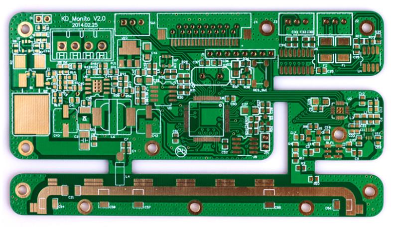
2. Introduction to PCB board process entry in PROTEL
Many beginners feel that the Protel software itself is easy to learn and easy to use, but some concepts and terms outside the software are more difficult to understand. In order to promote this powerful EDA tool, the software's manuals, etc. have been published in China, but unfortunately, these readings are often written for the software usage itself, which is confusing to readers in the PCB board process. There is little explanation of the concept. In order to design a board pattern that meets the requirements, you must first understand the general process flow of modern printed circuit boards, otherwise it will be a closed door. Generally speaking, printing boards are divided into single-sided, double-sided and multi-layer boards. The process of single-sided printing plate is relatively simple, usually blanking - screen printing - corrosion - removing printing material - hole processing - printing mark - coating flux - finished product. The process of multi-layer printing board is more complicated, namely: inner layer material processing - positioning hole processing - surface cleaning treatment - making inner layer wiring and pattern - corrosion - pre-lamination treatment - outer and inner layer material layer Pressing - Hole Processing - Hole Metallization - Making Outer Layer Graphics - Plating Corrosion Resistant Solderable Metals - Removing Photosensitive Adhesive - Corrosion - Plug Gold Plating - Shape Processing - Hot Melting - Coating Flux - finished product. The process complexity of the double-sided panel is between the two, and will not be described here.
2.1 The concept of "Layer"
Different from the concept of "layer" introduced in word processing or many other software to realize the nesting and synthesis of images, texts, colors, etc., the "layer" of rotel is not virtual, but the real material of the printing plate itself. in each copper foil layer. Today, components due to electronic circuits are densely mounted. Due to special requirements such as anti-interference and wiring, the printed boards used in some newer electronic products not only have upper and lower sides for wiring, but also have interlayer copper foil that can be specially processed in the middle of the board. Most of the printing plate materials are more than 4 layers. Because these layers are relatively difficult to process, they are mostly used to set up power wiring layers with relatively simple traces (such as Ground Dever and Power Dever in software), and are often routed by filling large areas (such as ExternaI P1a11e and Fill in software). ). The surface layers in the upper and lower positions and the places where the intermediate layers need to be connected are communicated with the so-called "Via" mentioned in the software. With the above explanation, it is not difficult to understand the related concepts of "multi-layer pad" and "wiring layer setting". To give a simple example, many people have completed wiring, but only when they found out that many terminals of the connection have no pads, in fact, they ignored the concept of "layer" when they added the device library, and did not draw and encapsulate their own. The pad characteristics are defined as "multi-layer (Mulii-Layer). It should be reminded that once the number of layers of the printed board used is selected, be sure to turn off those unused layers, so as not to cause trouble and detours.
2.2 Via
In order to connect the lines between the layers, a common hole is drilled at the intersection of the wires that need to be connected at each layer, which is a via hole. In the process, a layer of metal is plated by chemical deposition on the cylindrical surface of the hole wall of the via to connect the copper foils to be connected in the middle layers, and the upper and lower sides of the via are made into ordinary pad shapes, which can be directly It can be connected to the upper and lower lines, or not connected. Generally speaking, there are the following principles for the processing of vias when designing circuits: (1) Use as few vias as possible. Once vias are selected, be sure to deal with the gaps between them and surrounding entities, especially those in the middle that are easily overlooked. The gap between the lines and the vias that are not connected to the vias in each layer can be automatically resolved by selecting the "on" item in the "Via Minimiz8tion" submenu if it is automatically routed. (2) The larger the required current carrying capacity, the larger the required via hole size, such as the via hole used to connect the power supply layer and the ground layer with other layers.
2.3 Overlay
In order to facilitate the installation and maintenance of the circuit, the required logo patterns and text codes are printed on the upper and lower surfaces of the printed board, such as component label and nominal value, component outline shape and manufacturer logo, production date, etc. When designing the content of the silk screen layer, many beginners only pay attention to the neat and beautiful placement of the text symbols, ignoring the effect of the actual PCB board. On the printed boards they designed, the characters were either blocked by components (such as rivet standoffs) or invaded the soldering area and were smeared on credit, and some marked the component numbers on adjacent components. All kinds of designs will give Assembly and maintenance bring great inconvenience. Correct silkscreen layer characters. The layout principle is: "No ambiguity, see the needle, beautiful and generous".
2.4 The particularity of SMD
The Protel package library has a large number of SMD packages, ie surface mount devices. In addition to the small size, the characteristics of this type of device are single-sided distribution of element pin holes. Therefore, when selecting this type of device, it is necessary to define the surface of the device to avoid "Missing Plns". In addition, the relevant text annotations of such components can only be placed along the surface of the component.
2.5 External Plane and Fill
As the names of the two, the network filling area is to process a large area of copper foil into a mesh, and the filling area only retains the copper foil completely. In the process of designing for beginners, the difference between the two is often not visible on the computer. It is because it is usually difficult to see the difference between the two, so when using it, you don't pay attention to the distinction between the two. It should be emphasized that the former has a strong effect of suppressing high-frequency interference in circuit characteristics, and is suitable for It is especially suitable for places where a large area is filled, especially when certain areas are used as shielding areas, partition areas or high-current power lines.
2.6 Pad
The pad is a common and important concept in PCB design, but it is easy for beginners to ignore its selection and correction, and use circular pads in the design. When selecting the pad type of a component, factors such as the shape, size, layout, vibration and heat conditions, and force direction of the component should be comprehensively considered. Protel gives a series of pads of different sizes and shapes in the package library, such as round, square, octagonal, round square and positioning pads, etc., but sometimes this is not enough and needs to be edited by yourself. For example, for the pads with heat, high force and high current, they can be designed into "teardrop-shaped". In the design of the row output transformer pin pads of the familiar color TV PCB, many manufacturers are is in this form. Generally speaking, in addition to the above mentioned principles, when editing pads by yourself, the following principles should also be considered: (1) When the shape is inconsistent in length, the difference between the width of the connection and the specific side length of the pad should not be too large; (2) ) It is often necessary to use pads with asymmetric lengths when routing between the leading corners of components; (3) The size of the pad holes of each component should be edited and determined according to the thickness of the component pins. The principle is that the size of the hole is larger than the diameter of the pin. Large 0.2- 0.4 mm.
2.7 Mask
These films are not only indispensable in the PCB manufacturing process, but also a necessary condition for component soldering. According to the position and function of the "film", the "film" can be divided into two parts: the component surface (or welding surface) solder flux film (TOp or Bottom and the component surface (or welding surface) solder mask (TOp or BottomPaste Mask). Class. As the name suggests, the solder flux film is a layer of film applied to the pad to improve the solderability, that is, the light-colored circular spots on the green board that are slightly larger than the pad. The situation of the solder mask is just the opposite, in order to To adapt the manufactured board to welding forms such as wave soldering, it is required that the copper foil on the non-pad part of the board cannot stick to tin. Therefore, a layer of paint should be applied to all parts other than the pad to prevent tin from being applied to these parts. It can be seen that these two kinds of membranes are a complementary relationship. From this discussion, it is not difficult to determine the settings of items such as "solder Mask En1argement" in the menu.
2.8 Flying line, flying line has two meanings:
(1) A rubber band-like network connection for observation during automatic routing. After the components are loaded through the network table and a preliminary layout is made, the "Show command" can be used to see the crossover status of the network connection under the layout., Continuously adjust the position of the components to make this crossover less, so as to obtain the routing rate of the automatic routing. This step is very important, it can be said that the sharpening of the knife does not cut the firewood by mistake, spend more time, it is worth! In addition, the automatic routing is over, and which networks have not yet been deployed, you can also use this function to find out. After finding out the network that has not been deployed, manual compensation can be used. If it cannot be compensated, the second meaning of "flying line" should be used, which is in the future. These nets are connected by wires on the board. To be clear, if the board is a high-volume automatic wire production, this flying lead can be designed as a 0 ohm resistance element with uniform pad spacing.
3. Printing plate production process
Board-making process: trim the peripheral size of the board--replication--drilling positioning--gluing--corrosion--cleaning--degumming--fine sandpaper polishing--coating with rosin.
3.1 First, polish the surface of the copper-clad board that meets the size requirements with fine sandpaper, and then copy the wiring diagram to the copper-clad board with carbon paper.
3.2 Use a 1.0mm diameter drill to drill holes and locate the openings, and then glue (or paint).
3.3 After the glue is applied, a thick sheet should be placed on the board and pressed with the palm of the hand, the purpose is to make all the glue and the copper-clad board stick more firmly. If necessary, it can also be heated with a hair dryer, and the viscosity of the adhesive can be strengthened. Because the adhesive used is very sticky and the adhesive paper is thin, it is better to use this type of adhesive to make boards. Generally, it is No further heat treatment is required.
3.4 Ferric chloride is generally used as the corrosion solution for corrosion. The corrosion speed is related to the concentration of the corrosion solution, temperature and vibration during the corrosion process. In order to ensure the quality of the plate and improve the corrosion speed, the vibration and heating methods can be used.
3.5 After the corrosion is completed, it should be rinsed with tap water, the adhesive tape should be removed, and the printing plate should be wiped dry.
3.6. Wipe the copper-clad surface of the printed board with a fine emery cloth until it is bright, and then apply the rosin solution immediately. (When applying rosin, the printed circuit boards should be tilted and then applied with rosin to prevent the rosin from flowing to the back through the drilled holes).