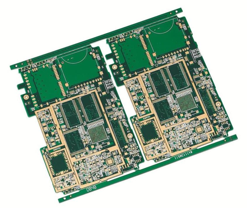
Analyze the routing strategy in high-speed PCB board design: A differential pair works by making the received signal equal to the difference between two complementary and referenced signals, thus greatly reducing the effects of electrical noise on the signal. The working principle of the single-ended signal is that the received signal is equal to the difference between the signal and the power supply or ground, so the noise on the signal or power supply system cannot be effectively canceled. This is why differential signaling is so effective for high-speed signaling, and why it is used in fast serial buses and double-data-rate memory.

In a differential pair, both positive and negative sides must always travel along the transmission path in the same environment. The positive and negative sides must be close together so that the positive and negative signals are coupled to each other via the electromagnetic fields at corresponding points on these signals. Differential pairs are symmetrical, so their environment must also be symmetrical. Of course, perfect symmetry is impossible, because at least there are dimensional tolerances. But designers can still achieve near-ideal differential signaling results if they follow some basic rules.
Make sure the signal is present at the same point on each line at the same time. Make the segments of the trace the same length, as indicated by the same letters in the figure. If the differential pair has series termination resistors or common-mode filters, these devices should be connected equally from the positive and negative pins of the differential driver. Route point-to-point, keeping the stub or branch (C in the diagram) within 0.6Tr inches in all cases, where Tr is the driver output rise time. A and E in the figure should use the same length limit rules as much as possible. Use a field solver to design trace spacing so that even-mode and odd-mode impedance values can be easily obtained. A 50 ohm board doesn't mean that the even-mode, odd-mode, or differential characteristic impedance is also 50 ohms. If a differential signal is to be terminated to ground or to a reference voltage, the effects of the harmful noise-contaminated environment and the odd-mode impedance should be considered. Termination of even-mode or common-mode (half the even-mode value) should also be considered to terminate unwanted noise. If terminating between two wires, the differential mode impedance (twice the odd mode impedance) should be considered. Remember that radiated noise from the same source can only be effectively suppressed if the differential pairs are tightly coupled, because the surrounding electromagnetic fields are likely to be nearly identical only when the traces are very close to each other. Extending trace lengths to compensate for any skew between complementary output signals is done close to the driver. Extend trace lengths only differentially as much as possible, remembering that the amount and style of left and right bends should be balanced.
Replacing odd- and even-mode impedances with single-ended characteristic impedances as termination impedances: Tightly coupled differential pairs are specifically designed for complementary signals. Just make sure that the total length of the trace is equal, not that every segment of the trace is equal. Differential pairs are routed across gaps in power or ground planes. Forgetting to define differential pairs when using the autorouting tool, you only get single-ended routing. Have the test engineer add test pads at different locations on each side of the differential pair. The test pad acts as an input to a high-impedance device, so it is easy to unbalance the differential pair. Other signals that are routed too parallel to the differential pair, or on another layer just below or above, can create crosstalk that can unbalance the differential signal. Route differential pairs above or below unrelated power or ground planes, such as separate analog power planes. Forgot to consider where the off-board connections go. When examining the target circuit with simulation, the connectors, cables, and differential topology on other boards in the system should be modeled. Blinded by the parasitic inductance and capacitance of the probe or test equipment. Placing a probe on one side of a differential pair will likely unbalance the differential pair, making the measurement easily misleading and the device likely to falsely fail under this test condition on PCB board.