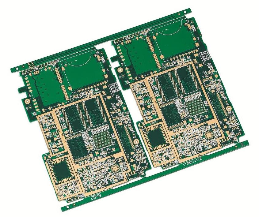
1. The concept of "Layer"
Due to special requirements such as anti-interference and wiring, the PCB board used in some newer electronic products, not only has upper and lower sides for wiring but also has interlayer copper foils that can be specially processed in the middle of the board, such as those used in current computer motherboards. Most of the printing plate materials are more than 4 layers. Because these layers are relatively difficult to process, they are mostly used to set up power wiring layers with relatively simple traces (such as Ground Dever and Power Dever in software) and are often routed by filling large areas (such as ExternaI P1a11e and Fill in software). ). The surface layers in the upper and lower positions and the places where the intermediate layers need to be connected are communicated with the so-called "Via" mentioned in the software. With the above explanation, it is not difficult to understand the related concepts of "multi-layer pad" and "wiring layer setting". To give a simple example, many people have completed the wiring, but only when they found out that many terminals of the connection have no pads, in fact, they ignored the concept of "layer" when they added the device library and did not draw and encapsulate their own. The pad characteristics are defined as "multi-layer (Multi-Layer). It should be reminded that once the number of layers of the printed board used is selected, be sure to turn off those unused layers, so as not to cause trouble and detours.

2. Via
In order to connect the lines between the layers, a common hole is drilled at the intersection of the wires that need to be connected at each layer, which is a via hole. In the process, a layer of metal is plated on the cylindrical surface of the hole wall the via chemical deposition to connect the copper foils that need to be connected between the layers in the middle, and the upper and lower sides of the via are made into ordinary pad shapes, which can be directly It can be connected to the upper and lower lines, or not connected. Generally speaking, there is the following principles for the processing of vias when designing circuits: (1) Use via as few as possible, once a via hole is selected, be sure to handle the gap between it and surrounding entities, especially the gap between the lines and via holes that are easily overlooked in the middle layers that are not connected to the via holes. Select the "on" item in the Via Minimiz8tion submenu to resolve automatically. (2) The larger the required current carrying capacity, the larger the required via hole sizes, such as the via hole used to connect the power supply layer and the ground layer with other layers.
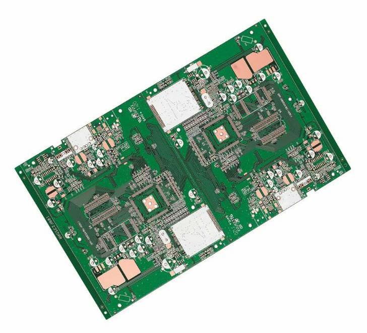
3. Silkscreen layer (Overlay)
In order to facilitate the installation and maintenance of the circuit, the required logo patterns and text codes are printed on the upper and lower surfaces of the printed board, such as component label and nominal value, component outline shape and manufacturer logo, and production date, etc. When designing the content of the silkscreen layer, many beginners only pay attention to the neat and beautiful placement of the text symbols, ignoring the effect of the actual PCB board. In the printed boards they designed, the characters were either blocked by the components or invaded the soldering area and were smeared on credit, and some marked the component numbers on the adjacent components. Such various designs will bring great benefits to assembly and maintenance. inconvenient. The principle of the correct character layout of the silkscreen layer is: "No ambiguity, see the seam and insert the needle, and be beautiful and generous".
4. The particularity of SMD
The Protel package library has a large number of SMD packages, ie surface mount devices. In addition to the small size, the characteristics of this type of device are the single-sided distribution of element pin holes. Therefore, when selecting this type of device, it is necessary to define the surface of the device to avoid "Missing Plus". In addition, the relevant text annotations of such components can only be placed along the surface of the component.
5. Grid-like filling area (External Plane) and filling area
As the names of the two, the network filling area is to process a large area of copper foil into a mesh, and the filling area only retains the copper foil completely. In the process of designing for beginners, the difference between the two is often not visible on the computer. It is because it is usually difficult to see the difference between the two, so when using it, you don't pay attention to the distinction between the two. It should be emphasized that the former has a strong effect of suppressing high-frequency interference in circuit characteristics, and is suitable for It is especially suitable for places where large areas are filled, especially when certain areas are used as shielding areas, partition areas or high-current power lines. The latter is mostly used in places where small areas need to be filled, such as general line ends or turning areas.
6. Pad
The pad is a common and important concept in PCB design, but it is easy for beginners to ignore its selection and correction, and use circular pads in the design. When selecting the pad type of a component, factors such as the shape, size, layout, vibration and heat conditions, and force direction of the component should be comprehensively considered. Protel gives a series of pads of different sizes and shapes in the package library, such as round, square, octagonal, round square and positioning pads, etc., but sometimes this is not enough and needs to be edited by yourself. For example, for the pads with heat, high force, and high current, they can be designed into "teardrop-shaped". In the design of the row output transformer pin pads of the familiar color TV PCB, many manufacturers are is in this form. In general, when editing pads by yourself, in addition to the above, the following principles should also be considered:
1) When the length of the shape is inconsistent, it should be considered that the difference between the width of the connection and the length of the specific side of the pad should not be too large;
2) It is often necessary to use pads with asymmetric lengths when routing between component leads;
3) The size of each component pad hole should be edited and determined according to the thickness of the component pins. The principle is that the size of the hole is 0.2-0.4 mm larger than the diameter of the pin.
7. Various types of film
These films are not only indispensable in the PCB manufacturing process, but also a necessary condition for component soldering. According to the position and function of the "film", the "film" can be divided into two parts: the component surface (or welding surface) solder flux film (Top or Bottom and the component surface (or welding surface) solder mask (TOp or BottomPaste Mask). Class. As the name suggests, the solder flux film is a layer of film applied to the pad to improve the solderability, that is, the light-colored circular spots on the green board that are slightly larger than the pad. The situation of the solder mask is just the opposite, in order to adapt the manufactured board to welding forms such as wave soldering, it is required that the copper foil on the non-pad part of the board cannot stick to the tin. Therefore, a layer of paint should be applied to all parts other than the pad to prevent tin from being applied to these parts. It can be seen that these two membranes are in a complementary relationship. From this discussion, it is not difficult to determine the settings of items such as "solder Mask En1argement" in the menu.
8. Flying line, the flying line has two meanings:
1) The network connection similar to a rubber band is used for observation during automatic routing. After the components are loaded through the network table and the preliminary layout is made, the "Show command" can be used to see the cross-state of the network connection under the layout. Continuously adjust the position of the components to make this crossover less, so as to obtain the routing rate of the automatic routing. This step is very important. It can be said that it is a good way to sharpen the knife without accidentally cutting firewood. It is worth spending more time! In addition, the automatic routing is over, You can also use this function to find out which networks have not yet been deployed. After finding out the networks that have not been deployed, manual compensation can be used. These nets are connected by wires on the board. To be clear, if the PCB board is a high-volume automatic wire production, this flying lead can be designed as a 0-ohm resistance element with uniform pad spacing.