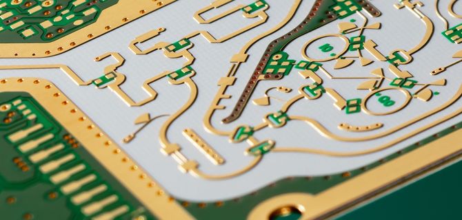
New UV laser processing technology for PCB board and substrate
Since the ablation limit of epoxy is lower than that of copper (yellow), the cleaning step (green) cannot penetrate into the underlying copper. The beam is softly illuminated, balancing material thickness and uniform tolerances.
Develop HDIs Via Process by UV:
Process A: 4-step process, mixed wetting, and laser processes mask tolerances are between 50 and 70im, and typical hole sizes are 100 to 125im.
Process B: 2-step laser process, 1-step wetting process, due to the diffraction of CO2 on the mask, the diameter of the small hole is about 60im. The limit of copper opening thickness that can be provided for the specially treated copper material CO2 is 7im. This process still needs to remove the smudge.
C process: 1-step laser process, UV laser has no restrictions on the drilling of inner and outer copper, and UV has an additional cleaning process, which reduces the drilling contamination process to a limit, and can even replace the drilling contamination process.

UV lasers have the ability to reduce a complete hole process step to a single laser step, especially eliminating the need for de-drilling or even eliminating this step entirely, especially for pulse pattern plating. There is no need to use aggressive besmearing procedures, such as for CO2 lasers, hole shape roughness, wicking, and barrel distortion are improved.
Other applications and quality results of UV lasers
Blind hole
Double layer vias
through hole
Flexible
The new laser system can perform complex drawing operations in addition to the commonly used focused irradiation operation in the hole, which can be used to cut thin line patterns or to remove solder mask after buried mask. Almost any shape of the machining area can be processed. So far, when the defects on the solder mask are just some minor faults and insignificant, the laser ablation of the solder mask is only used to repair some damaged pads, so that the whole panel will not be scrapped, but HDI technology requires more opening size and positioning. The figure below shows the circular and square solder mask openings and cross-sections formed after pressure steam testing and thermal cycling. With speeds up to 100+ pads per second, for BGA and FC, the cost of 128 pads per IC is about 0.5 cents. When drawing thin lines, the graphics are engraved by the laser track, as shown in the figure below, the speed of the laser track can reach 1000mm/s. After laser ablation of 1im thick tin, the width is between 15~25im. After the tin pattern is drawn, the pattern is etched, maintaining the spacing of the laser's track width and the side effects of etching. For copper with a thickness of 12im, a pattern of less than 2mil/2mil can be obtained. Fan-out for IC and MCM patterns of 2mil/2mil structure. The application of directly drawing thin line graphics is limited by the drawing speed. The fan-out as shown in the figure below takes less than 1 second, while the fan-out of a complete graphic in an area of 40×40mm takes 10 to 15 seconds.
Conclusion
UV laser systems provide a complementary solution to existing CO2 drilling tools. Short wavelengths and small spots allow for greater flexibility and greater complexity for drilling. The goal of UV lasers is more to meet the needs of HDI. Compared with CO2 performance, especially for macropores, there is still a gap in UV output, but with the development of high-power and high-frequency UV lasers, this difference will become smaller and smaller. The number of processing steps to generate vias with a UV laser will be reduced to a single laser step, and the required besmearing steps will be minimized. In addition to its primary drilling use, UV systems can also be used for direct drawing and precision ablation of solder masks. This provides added value to UV lasers. There is still plenty of room to improve UV laser systems in terms of throughput. Smaller pulse widths, high frequencies, higher power, and high-speed servo operation will all increase productivity, and in the near future, the market will increasingly accept UV laser systems as a complete tool on PCB board.