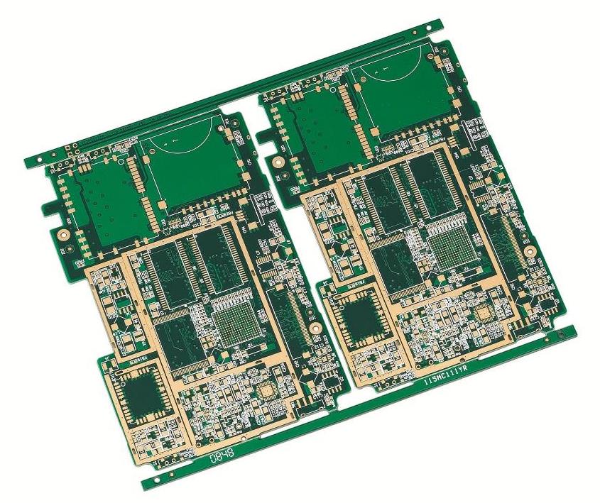
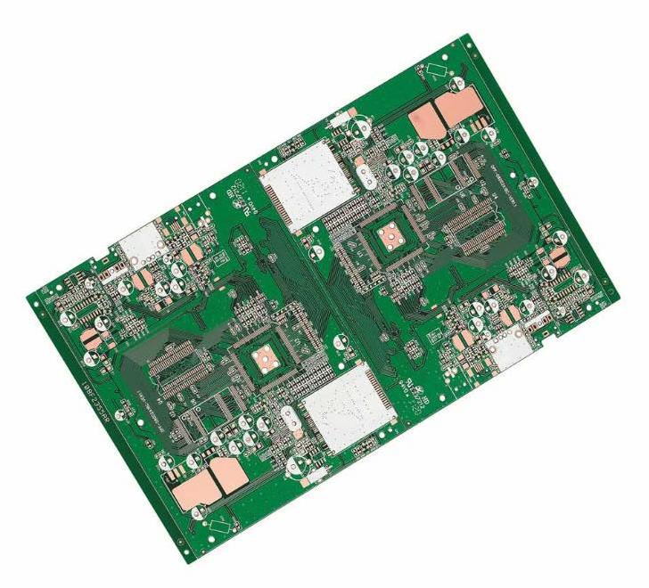
PCB board supports circuit components and devices in electronic products. It provides electrical connections between circuit elements and devices. With the rapid development of electrical technology, the density of PGB is getting higher and higher. The quality of the PCB board design has a great impact on the ability to resist interference. Therefore, when designing the PCB board. The general principles of PCB board design must be followed, and the requirements for anti-interference design should be met. The general principle of PCB board design is to obtain the performance of electronic circuits, the layout of components and the layout of wires are very important. In order to design a PCB board with good quality and low cost.

1. Layout First, consider the size of the PCB board. When the size of the PCB board is too large, the printed lines will be long, the impedance will increase, the anti-noise ability will decrease, and the cost will increase; if the size is too small, the heat dissipation will be poor, and the adjacent lines will have easily interfered. After determining the size of the PCB board. Then determine the location of special components. , according to the functional unit of the circuit, the layout of all the components of the circuit. Observe the following guidelines when locating special components:
1) Shorten the connection between high-frequency components as much as possible, and try to reduce their distribution parameters and mutual electromagnetic interference. Components that are susceptible to interference should not be too close to each other, and input and output components should be kept as far apart as possible.
2) There may be a high potential difference between some components or wires, and the distance between them should be increased to avoid accidental short circuits caused by the discharge. Components with high voltage should be arranged as far as possible in places that are not easily accessible by hand during debugging.
3) Components weighing more than 15g should be fixed with brackets and then welded. Those components that are large, heavy, and generate a lot of heat should not be installed on the printed board but should be installed on the chassis bottom plate of the whole machine, and the heat dissipation problem should be considered. Thermal elements should be kept away from heating elements.
4) For the layout of adjustable components such as potentiometers, adjustable inductance coils, variable capacitors, and micro switches, the structural requirements of the whole machine should be considered. If it is adjusted inside the machine, it should be placed on the printed board where it is convenient for adjustment; if it is adjusted outside the machine, its position should be adapted to the position of the adjustment knob on the chassis panel.
5) The position occupied by the positioning hole of the printed pulley and the fixing bracket should be reserved. According to the functional unit of the circuit. When laying out all the components of the circuit, the following principles should be followed:
Arrange the position of each functional circuit unit according to the circuit flow, so that the layout is convenient for signal circulation, and the signal keeps the same direction as possible.
b Layout around each functional circuit element centered on it. Components should be arranged evenly, neatly, and compactly on the PCB. Minimize and shorten leads and connections between components.
c For circuits that work at high frequencies, the distribution parameters between components should be considered. In general circuits, the components should be arranged in parallel as much as possible. This is not only beautiful. And it is easy to install and weld. Easy to mass-produce.
d The components located on the edge of the circuit board are generally not less than 2mm away from the edge of the circuit board. The shape of the circuit board is rectangular. The aspect ratio is 3:2 to 4:3. When the size of the circuit board is larger than 200x150mm. Consideration should be given to the mechanical strength experienced by the circuit board.
2. Wiring;
1) The wires used at the input and output terminals should avoid being adjacent and parallel as much as possible. Add ground wire between wires to avoid feedback coupling.
2) The width of the printed wire is mainly determined by the adhesion strength between the wire and the insulating base plate and the value of the current flowing through them. When the copper foil thickness is 0.05mm and the width is 1~15mm. With a current of 2A, the temperature will not be higher than 3°C, so. The wire width of 1.5mm can meet the requirements. For integrated circuits, especially digital circuits, a wire width of 0.02~0.3mm is usually selected. Of course, use as wide a line as possible whenever possible. Especially the power and ground wires. The spacing of the wires is mainly determined by the wire-to-wire insulation resistance and breakdown voltage under bad conditions. For integrated circuits, especially digital circuits, as long as the process allows, the spacing can be as small as 5~8mm.
3) The corners of printed conductors are generally arc-shaped, and right angles or included angles will affect electrical performance in high-frequency circuits. In addition, try to avoid the use of large-area copper foil, otherwise, the copper foil will easily expand and fall off when heated for a long time. When a large area of copper foil must be used, use a grid. This is beneficial to eliminate the volatile gas generated by the heating of the adhesive between the copper foil and the substrate.
3. The center hole of the pad is slightly larger than the diameter of the device lead. If the pad is too large, it is easy to form a virtual solder. The outer diameter D of the pad is generally not less than (d+1.2) mm, where d is the lead hole diameter. For high-density digital circuits, the diameter of the pad may be (d+1.0) mm. Anti-interference measures for PCB boards and circuits The anti-interference design of printed circuit boards is closely related to specific circuits.
3.1 Power line design According to the size of the printed circuit board current, try to increase the width of the power line to reduce the loop resistance. At the same time, make the direction of the power line and the ground line consistent with the direction of data transmission, which will help to enhance the anti-noise capability.
3.2 Lot design The principles of ground line design are:
1) Separate digital ground from the analog ground. If there are logic circuits and linear circuits on the circuit board, they should be separated as much as possible. The ground of the low-frequency circuit should be grounded in parallel at a single point as far as possible. When the actual wiring is difficult, it can be partially connected in series and then grounded in parallel. The high-frequency circuit should be grounded at multiple points in series, the ground wire should be short and leased, and the large-area grid-shaped ground foil should be used around the high-frequency components as much as possible.
2) The ground wire should be as thick as possible. If the ground wire is very slender, the ground potential will change with the change of the current, which will reduce the anti-noise performance. Therefore, the ground wire should be thickened so that it can pass three times the allowable current on the printed board. If possible, the ground wire should be more than 2~3mm.
3) The ground wire forms a closed loop. For printed boards composed only of digital circuits, most of the grounding circuits are arranged in a loop, which can improve the anti-noise ability.
3.3 Decoupling capacitor configuration One of the conventional practices in PCB board design is to configure appropriate decoupling capacitors in each key part of the printed board. The general configuration principles of decoupling capacitors are:
1) Connect an electrolytic capacitor of 10 ~ 100uf across the power input. If possible, it is better to connect with more than 100uF.
2) In principle, each integrated circuit chip should be arranged with a 0.01pF ceramic capacitor. If the printed board space is not enough, a 1 ~ 10pF capacitor can be arranged every 4~8 chips.
3) For devices with weak anti-noise capability and large power changes when turned off, such as RAM and ROM storage devices, a decoupling capacitor should be directly connected between the power line and the ground line of the chip.
4) The lead wire of the capacitor should not be too long, especially the high-frequency bypass capacitor should not have a lead wire. In addition, the following two points should also be noted: when there are contactors, relays, buttons, and other components on the PCB board.