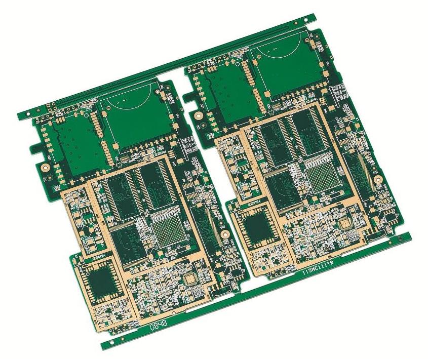
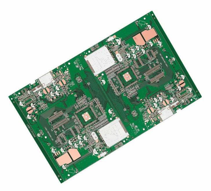
With the development of communication technology, handheld wireless radio frequency PCB board technology is used more and more widely, such as wireless pager, mobile phone, wireless PDA, etc. The performance index of the radio frequency circuit directly affects the quality of the whole product. One of the characteristics of these handheld products is miniaturization, and miniaturization means a high density of components, which makes the mutual interference of components (including SMD, SMC, bare chips, etc.) very prominent. Improper handling of electromagnetic interference signals may cause the entire circuit system to fail to work properly. Therefore, how to prevent and suppressing electromagnetic interference and improving electromagnetic compatibility have become very important issues when designing RF circuit PCB boards. The same circuit, different PCB board design structure, its performance index will be very different. In this discussion, when Protel99 SE software is used to design the RF circuit PCB board of handheld products, if the performance indicators of the circuit are realized to the maximum extent, in order to meet the requirements of electromagnetic compatibility.
1. Selection of plates
The substrates of printed circuit boards include two categories: organic and inorganic. The important properties in the substrate are dielectric constant εr, dissipation factor (or dielectric loss) tanδ, thermal expansion coefficient CET, and moisture absorption rate. Among them, εr affects the circuit impedance and the signal transmission rate. For high-frequency circuits, permittivity tolerance is a more critical factor to consider first, and a substrate with a small permittivity tolerance should be selected.

2. PCB board design process
Since the use of Protel99 SE software is different from that of Protel98 and other software, first, the process of PCB board design using Protel99 SE software is briefly discussed.
1) Since Protel99
SE adopts the project database mode management, which is implicit under Windows 99, so you should first set up a database file to manage the designed circuit schematic diagram and PCB board layout.
2) The design of the schematic diagram. In order to realize the network connection, the components used must exist in the component library between the principle design, otherwise, the required components should be made in SCHLIB and stored in the library file. Then, just call the required components from the component library and connect them according to the designed circuit diagram.
3) After the schematic design is completed, a netlist can be formed for use in PCB board design.
4) PCB board design.
a Determination of the shape and size of the PCB board. The shape and size of the PCB board are determined according to the position of the designed PCB board in the product, the size and shape of the space, and the cooperation with other components. Use the PLACE TRACK command to draw the outline of the PCB on the MECHANICAL LAYER layer.
b According to the requirements of SMT, make positioning holes, eyes, reference points, etc. on the PCB board.
c The production of components. If you need to use some special components that do not exist in the component library, you need to make the components before the layout. The process of making components in Protel99 SE is relatively simple. After selecting the "MAKE LIBRARY" command in the "DESIGN" menu, you will enter the component-making window, and then select the "NEW COMPONENT" command in the "TOOL" menu. device design. At this time, you only need to draw the corresponding pads at a certain position on the TOP LAYER layer with commands such as PLACE PAD according to the shape and size of the actual components and edit them into the required pads (including the shape, size, and inner diameter of the pads). In addition, the corresponding pin name of the pad should be marked), and then use the PLACE TRACK command to draw the shape of the component in the TOP OVERLAYER layer, and take a component name and store it in the component library.
d After the components are made, the layout and wiring are carried out. These two parts are discussed in detail below.
e Inspection must be carried out after the above process is completed. On the one hand, it includes the inspection of the circuit principle, and on the other hand, it must also check the mutual matching and assembly problems. The circuit principle can be checked manually, or it can be checked automatically by the network (the network formed by the schematic diagram can be compared with the network formed by the PCB board).
f After checking that it is correct, archive and output the file. In Protel99 SE, you must use the "EXPORT" command in the "FILE" option to store the file in the specified path and file (the "IMPORT" command is to transfer a file into Protel99 SE). Note: After the "SAVE COPY AS..." command in the "FILE" option in Protel99 SE is executed, the selected file name is not visible in Windows 98, so the file cannot be seen in the resource manager. This is not exactly the same as the "SAVE AS..." function in Protel 98.
3. Layout of components
Since SMT generally uses infrared furnace heat flow welding to realize the welding of components, the layout of components affects the quality of solder joints, which in turn affects the yield of products. For RF circuit PCB board design, electromagnetic compatibility requires that each circuit module does not generate electromagnetic radiation as much as possible, and has a certain ability to resist electromagnetic interference. Therefore, the layout of components also directly affects the interference and anti-interference of the circuit itself. capability, which is also directly related to the performance of the designed circuit. Therefore, in addition to considering the layout of ordinary PCB board design when designing a RF circuit PCB, it is also necessary to consider how to reduce the mutual interference between various parts in the RF circuit, how to reduce the interference of the circuit itself to other circuits, and The anti-interference ability of the circuit itself. According to experience, the effect of the RF circuit depends not only on the performance indicators of the RF circuit board itself but also on the interaction with the CPU processing board. Therefore, when designing the PCB board, a reasonable layout is particularly important. . The general principle of layout: components should be arranged in the same direction as possible, and the phenomenon of poor soldering can be reduced or even avoided by selecting the direction in which the PCB board enters the tin melting system; Tin requirements, if the space of the PCB board allows, the spacing of components should be as wide as possible. For double-sided panels, one side should generally be designed with SMD and SMC components, and the other side should be discrete components. The layout should pay attention to:
1) First determine the position of the interface components with other PCB boards or systems on the PCB board, and you must pay attention to the coordination between the interface components (such as the direction of the components, etc.).
2) Because the size of the handheld products is very small, and the components are arranged in a compact manner, the larger components must be given priority, the corresponding positions must be determined, and the cooperation between them must be considered.
3) Carefully analyze the circuit structure, process the circuit in blocks (such as high-frequency amplifier circuit, frequency mixing circuit and demodulation circuit, etc.), separate strong electric signals and weak electric signals as much as possible, and separate digital signal circuits and analog signal circuits. , the circuits that complete the same function should be arranged within a certain range as much as possible, thereby reducing the signal loop area; the filter network of each part of the circuit must be connected nearby, which can not only reduce radiation but also reduce the probability of being interfered. The anti-interference ability of the circuit.
4) According to the different sensitivity of the unit circuit to electromagnetic compatibility in use, it is grouped. For the components that are susceptible to interference in the circuit, the layout should also try to avoid interference sources (such as interference from the CPU on the data-processing board, etc.).
4. Wiring
After the layout of the components is basically completed, the wiring can be started. The basic principle of wiring is: after the assembly density permits, try to use a low-density wiring design, and the thickness of the signal traces should be as consistent as possible, which is conducive to impedance matching. For RF circuits, the unreasonable design of the direction, width, and line spacing of signal lines may cause cross-interference between signal and signal transmission lines; in addition, the system power supply itself also has noise interference, so it must be integrated when designing the RF circuit PCB board. Consider, reasonable wiring. When wiring, all traces should be kept away from the frame of the PCB board (about 2mm), so as to avoid the possibility of disconnection or potential disconnection during the production of the PCB board. The power line should be as wide as possible to reduce the loop resistance. At the same time, the direction of the power line and the ground line should be consistent with the direction of data transmission to improve the anti-interference ability; the signal line should be as short as possible, and minimize excessive The number of holes; the connection between the components is as short as possible to reduce the distribution parameters and mutual electromagnetic interference; for incompatible signal lines should be far away from each other, and try to avoid parallel lines, and on both sides of the positive The signal lines should be perpendicular to each other; when wiring, the address side that needs a corner should be at a 135° angle, and a right angle should be avoided. When wiring, the lines directly connected to the pads should not be too wide, and the traces should be kept away from the disconnected components as much as possible to avoid short circuits; the vias should not be drawn on the components, and should be kept away from the disconnected components as much as possible to avoid production. There are phenomena such as virtual welding, continuous welding, and short circuit. In the design of the RF circuit PCB board, the correct wiring of the power line and the ground line is particularly important, and a reasonable design is an important means to overcome electromagnetic interference. Quite a lot of interference sources on the PCB board are generated by the power supply and the ground wire, among which the noise interference is caused by the ground wire. The main reason why the ground wire is prone to electromagnetic interference is that the ground wire has impedance. When there is currently flowing through the ground wire, a voltage will be generated on the ground wire, resulting in a ground wire loop current and a ground wire loop interference. When multiple circuits share a ground wire, common impedance coupling is formed, resulting in so-called ground wire noise. Therefore, when wiring the ground wire of the RF circuit PCB board, you should do:
1) First, the circuit is divided into blocks. The radio frequency circuit can basically be divided into high-frequency amplification, frequency mixing, demodulation, local oscillator, and other parts. It is necessary to provide a common potential reference point for each circuit module, that is, the respective ground of each module circuit. lines so that signals can be transmitted between different circuit modules. Then, it is summarized in the place where the RF circuit PCB board is connected to the ground wire, that is, it is summarized in the general ground wire. Since there is only one reference point, there is no common impedance coupling and therefore no mutual interference problems.
2) The digital area and the analog area should be isolated from the ground as much as possible, and the digital ground and the analog ground should be separated and connected to the power ground.
3) The ground wire inside each part of the circuit should also pay attention to the principle of single-point grounding, minimize the area of the signal loop, and connect it with the address of the corresponding filter circuit nearby.
4) When space allows, each module can be isolated by a ground wire to prevent the signal coupling effect between each other.
5 Conclusion
The key to the design of the RF circuit PCB is how to reduce the radiation ability and how improve the anti-interference ability. Reasonable layout and wiring are the guarantees for the design of the RF circuit PCB. The method described in this paper is beneficial to improve the reliability of the PCB board design of the radio frequency circuit, solve the problem of electromagnetic interference, and then achieve the purpose of electromagnetic compatibility.