1. Common mistakes in PCB board schematic diagrams:
(1) The ERC pin has no access signal:
a. I/O attributes are defined for the pins when the package is created;
b. The inconsistent grid properties were modified when creating components or placing components, and the pins and lines were not connected;
c. When creating a component, the pin direction is reversed, and it must be connected to the non-pin name end.
(2) The component runs out of the drawing bounds: The component is not created in the center of the drawing paper of the component library.
(3) The created project file netlist can only be partially transferred to the PCB board: global is not selected when the netlist is generated.
(4) Never use annotate when using self-created multi-part components.

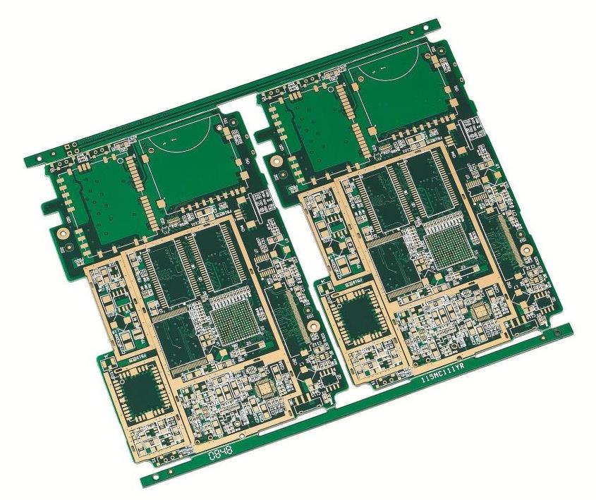
2. Common mistakes in PCB board:
(1) NODE is not found when the network is loaded:
a. The components in the schematic diagram use packages that are not in the PCB library;
b. The components in the schematic diagram use packages with inconsistent names in the PCB library;
c. The components in the schematic diagram use packages with inconsistent pin numbers in the PCB library. Such as triode: the pin number in sch is e,b,c, while in the PCB board it is 1, 2, 3.
(2) When printing, it cannot always be printed on one page:
a. It is not at the origin when creating the PCB library;
b. The component has been moved and rotated many times, and there are hidden characters outside the PCB board boundary. Select to show all hidden characters, shrink the PCB board, and move the characters within the boundaries.
(3) The DRC network is divided into several parts:
Indicates that the network is not connected, look at the file, and use the CONNECTED COPPER to find it.
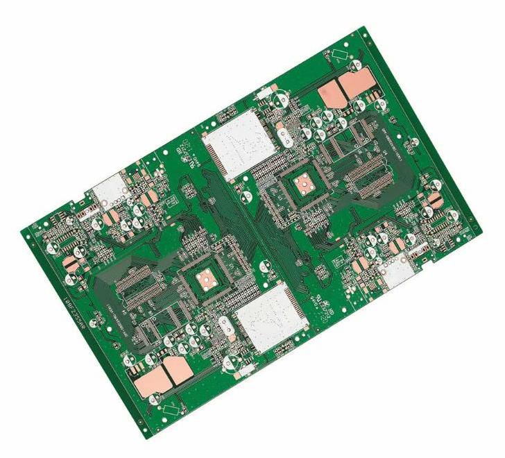
In PCB board design, wiring is an important step to complete product design. It can be said that the previous preparations are all done for it. In the entire PCB board, the wiring design process is limited, the skills are fine and the workload is. PCB board wiring includes single-sided wiring, double-sided wiring, and multi-layer wiring. There are also two ways of routing: automatic routing and interactive routing. Before automatic routing, you can use interactive pre-routing for the lines with stricter requirements. The edges of the input end and the output end should avoid being adjacent and parallel to avoid reflection interference. If necessary, ground wire isolation should be added, and the wiring of two adjacent layers should be perpendicular to each other, and parasitic coupling will easily occur in parallel. The routing rate of automatic routing depends on the good layout, and routing rules can be preset, including the number of bends of the routing, the number of vias, the number of steps, and the like. Generally, exploratory wiring is performed first, the short wires are quickly connected, and then the labyrinth wiring is performed. And try re-wiring to improve the overall effect.
3. Handling of power and ground wires
Even if the wiring in the entire PCB board is well completed, the interference caused by the lack of thoughtful consideration of the power supply and the ground wire will reduce the performance of the product, and sometimes even affect the success rate of the product. Therefore, the wiring of the power and ground wires should be taken seriously, and the noise interference generated by the power and ground wires should be minimized to ensure the quality of the product. Every engineer who is engaged in the design of electronic products understands the reason for the noise between the ground wire and the power line, and now only the reduced noise suppression is expressed: it is well known that the addition of the noise between the power supply and the ground wire coupling capacitor. Try to widen the width of the power supply and the ground wire. The ground wire is wider than the power supply wire. mm, the power cord is 1.2 to 2.5 mm. For the PCB board of the digital circuit, a wide ground wire can be used to form a loop, that is, a ground net can be used (the ground of the analog circuit cannot be used in this way). Use a large-area copper layer as a ground wire, and connect the unused places on the printed board to the ground as a ground wire. Or make a multi-layer board, power supply, and ground wire each occupy one layer.
4. Common ground processing of digital circuits and analog circuits
Now there are many PCB boards that are no longer a single function circuit (digital or analog circuit) but are composed of a mixture of digital and analog circuits. Therefore, it is necessary to consider the mutual interference between them when wiring, especially the noise interference on the ground wire. The frequency of the digital circuit is high, and the sensitivity of the analog circuit is strong. For the signal line, the high-frequency signal line should be kept away from the sensitive analog circuit devices as much as possible. For the ground line, the whole PCB board has only one node to the outside world. Therefore, the problem of digital and analog common ground must be dealt with inside the PCB board, while the digital ground and the analog ground are actually separated inside the board, and they are not connected to each other, only at the interface between the PCB board and the outside world (such as plugs). Wait). The digital ground is a little shorted from the analog ground, note that there is only one connection point. There are also different grounds on the PCB board, which are determined by the system design.
5. Signal lines are routed on the electrical (ground) layer
In the wiring of multi-layer printed boards, since there are not many lines left in the signal line layer, adding more layers will cause waste and increase the production workload, and the cost will increase accordingly. To solve this contradiction, we can consider wiring on the electrical (ground) layer. The power plane should be considered first, followed by the ground plane. Because the integrity of the formation is preserved.
6. Handling of connecting legs in large area conductors
In a large area of grounding (electricity), the legs of commonly used components are connected to it, and the handling of the connecting legs needs to be comprehensively considered. There are some hidden dangers in the welding assembly of components, such as 1) Welding requires high-power heaters. 2) It is easy to cause virtual solder joints. Therefore, taking into account the electrical performance and process needs, cross-shaped pads are made, which are called thermal isolation and are commonly known as thermal pads. In this way, the possibility of virtual solder joints caused by excessive heat dissipation of the cross-section during welding can be greatly reduced. The electrical (ground) leg of a multilayer PCB board is treated the same way.