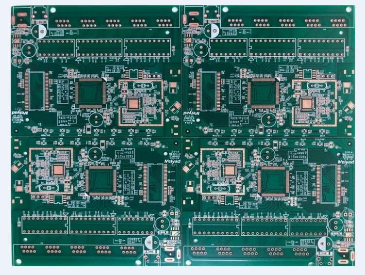
Vias are one of the important components of multi-layer PCB board, and the cost of drilling usually accounts for 30% to 40% of the cost of PCB board production. Simply put, every hole on a PCB can be called a via.
1. From the perspective of function, vias can be divided into two categories:
1) It is used as an electrical connection between layers;
2) It is used for fixing or positioning the device.
In terms of process, these vias are generally divided into three categories, namely blind vias, buried vias, and through vias.
Blind holes are located on the top and bottom surfaces of the printed circuit board, with a certain depth, for the connection of the surface circuit and the underlying inner circuit, and the depth of the hole usually does not exceed a certain ratio (diameter).
Buried vias refer to connection holes located in the inner layer of the printed circuit board, which do not extend to the surface of the circuit board. The above two types of holes are located in the inner layer of the circuit board and are completed by the through hole forming process before lamination. During the formation of the via hole, several inner layers may be overlapped.
The third type is called through-hole, which penetrates the entire circuit board and can be used for internal interconnection or as a mounting location hole for components. Because the through hole is easier to realize in the process and the cost is lower, most of the printed circuit boards use it instead of the other two kinds of through holes. The via holes mentioned below are considered as through holes unless otherwise specified. From a design point of view, a via is mainly composed of two parts, one is the drill hole in the middle, and the other is the pad area around the drill hole, as shown in the figure below. The size of these two parts determines the size of the via. Obviously, in the design of high-speed and high-density PCB boards, designers always hope that the smaller the via hole, the better, so that more wiring space can be left on the board. In addition, the smaller the via hole, the more parasitic capacitance of its own The smaller it is, the more suitable it is for high-speed circuits. However, the reduction in hole size also brings an increase in cost, and the size of the via hole cannot be reduced indefinitely. It is limited by process technologies such as drilling and plating: the smaller the hole, the more drilling The longer the hole takes, the easier it is to deviate from the center; and when the depth of the hole exceeds 6 times the diameter of the drilled hole, it is not guaranteed that the hole wall will be uniformly plated with copper. For example, the thickness of a normal 6-layer PCB board (through hole depth) is about 50Mil, so the diameter of the hole provided by the PCB board manufacturer can only reach 8Mil.

2. Parasitic capacitance of vias The vias themselves have parasitic capacitances to the ground. If it is known that the diameter of the isolation holes of the vias on the ground layer is D2, the diameter of the via pads is D1, and the thickness of the PCB board is T, The dielectric constant of the board substrate is ε, then the parasitic capacitance of the via is similar to: C=1.41εTD1/(D2-D1) The main impact of the parasitic capacitance of the via on the circuit is to prolong the rise time of the signal and reduce the speed of the circuit.
For example, for a PCB board with a thickness of 50Mil, if a via hole with an inner diameter of 10Mil and a pad diameter of 20Mil is used, and the distance between the pad and the ground copper area is 32Mil, we can approximate the via hole through the above formula. The parasitic capacitance is rough:
C=1.41x4.4x0.050x0.020/(0.032-0.020)=0.517pF,
The rise time change caused by this part of the capacitance is:
T10-90=2.2C(Z0/2)=2.2x0.517x(55/2)=31.28ps.
From these values, it can be seen that although the effect of the rise and delay caused by the parasitic capacitance of a single via is not very obvious, if the via is used multiple times in the trace to switch between layers, the designer should still consider carefully.
3. Parasitic inductance of vias Similarly, there are parasitic inductances along with parasitic capacitances of vias. In the design of high-speed digital circuits, the harm caused by parasitic inductances of vias is often greater than the influence of parasitic capacitances. Its parasitic series inductance will weaken the contribution of the bypass capacitor and reduce the filtering effect of the entire power system. We can easily calculate the approximate parasitic inductance of a via with the following formula: L=5.08h[ln(4h/d)+1]
where L is the inductance of the via, h is the length of the via, and d is the diameter of the center drilled hole. It can be seen from the formula that the diameter of the via hole has little effect on the inductance, while the length of the via hole affects the inductance. Still using the above example, the inductance of the via can be calculated as: L=5.08x0.050[ln(4x0.050/0.010)+1]=1.015nH. If the rise time of the signal is 1ns, then its equivalent impedance is XL=πL/T10-90=3.19Ω. Such impedance can no longer be ignored when high-frequency current passes through. It should be noted that the bypass capacitor needs to pass through two vias when connecting the power supply layer and the ground layer so that the parasitic inductance of the vias will be multiplied.
4. Via design in high-speed PCB board Through the above analysis of the parasitic characteristics of vias, we can see that in the design of high-speed PCB boards, seemingly simple vias often bring a lot to the circuit design. negative effects. In order to reduce the adverse effects caused by the parasitic effects of vias, you can try to do as much as possible in the design:
1) Considering both cost and signal quality, select a via the size of a reasonable size. For example, for 6-10 layer memory module PCB board design, it is better to use 10/20Mil (drilling/pad) vias. For some high-density small-sized boards, you can also try to use 8/18Mil. vias. Under current technical conditions, it is difficult to use smaller vias. For power or ground vias, consider using larger sizes to reduce impedance.
2) From the two formulas discussed above, it can be concluded that using a thinner PCB board is beneficial to reduce the two parasitic parameters of the via.
3) Try not to change the layers of the signal traces on the PCB, that is to say, try not to use unnecessary vias.
4) The pins of the power supply and ground should be drilled as close as possible. The shorter the lead between the via and the pin, the better, because they will increase the inductance. At the same time, the leads of power and ground should be as thick as possible to reduce impedance.
5) Place some grounded vias near the vias where the signal changes layers to provide a short return path for the signal. It is even possible to place a few redundant ground vias on the PCB in large numbers. Of course, flexibility is also required in the design. The via model discussed earlier in the case where each layer has pads, and sometimes, we can reduce or even remove the pads of some layers. Especially in the case of a very high density of vias, it may lead to the formation of a circuit breaker on the copper layer. To solve this problem, in addition to moving the position of the via, we can also consider placing the via on the copper layer. The pad size is reduced on PCB board.