Most of the current electronic PCB board designs are integrated system-level designs, and the entire project includes both hardware design and software development. This technical feature presents new challenges to electronic engineers. First, how to divide the system software and hardware functions reasonably in the early design stage to form an effective functional structure framework to avoid redundant cycle processes; second, how to design high-performance and high-reliability PCB boards in a short time. Because the development of software is largely dependent on the realization of hardware, the design cycle can be shortened more effectively only if the design of the whole machine is passed. This paper discusses the new features and new strategies of system board-level design under the new technical background. As we all know, the development of electronic technology is changing with each passing day, and the root of this change is mainly due to the advancement of chip technology. The semiconductor process is getting closer to the physical limit and has now reached the deep sub-micron level, and ultra-large-scale circuits have become the mainstream of chip development. And this process and scale change has brought many new electronic design bottlenecks throughout the electronics industry. The board-level design has also been greatly impacted. An obvious change is that the types of chip packages are extremely rich; secondly, high-density lead packaging and miniaturized packaging have become a fashion, in order to achieve the miniaturization of the whole product, such as Wide application of MCM technology. In addition, the improvement of the operating frequency of the chip makes it possible to increase the operating frequency of the system. And these changes inevitably bring many problems and challenges to board-level design. First, due to the increasing physical limits of high-density pins and pin sizes, resulting in low routing rates; second, due to the increase in system clock frequency, timing, and signal integrity issues; Complete complex, high-performance designs with better tools.

The design of high-speed digital circuits (ie, high clock frequencies and fast edges) has become mainstream. Product miniaturization and high performance must face the problem of distribution effects caused by mixed-signal design techniques (ie, digital, analog, and RF mixed design) on the same board. The increase in design difficulty makes the traditional design process and design method, as well as the CAD tools on the PC difficult to meet the current technical challenges. Therefore, the transfer of the EDA software tool platform from UNIX to the NT platform has become a trend recognized by the industry. In general, when the interconnect delay of the signal is greater than 20% of the edge signal flipping threshold time, the signal wire on the board will show the transmission line effect, that is, the connection is no longer a pure wire performance showing lumped parameters. Instead, it exhibits distributed parameter effects, and this design is a high-speed design. In high-speed digital system design, designers must address false inversions and signal distortion caused by parasitics—that is, timing and signal integrity issues. At present, this is also a bottleneck problem that high-speed circuit designers must solve. We can find that in traditional high-speed circuit design, electrical rule setting and physical rule setting are separate. This brings the following drawback: engineers have to spend a lot of effort in the early design stage to perform exhaustive front-end (ie, logic setup-physical implementation) analysis to plan a physical routing strategy that meets electrical requirements. The high-speed effect is a complex subject, and the desired effect cannot be achieved simply by controlling the wiring length and parallel lines. The designer is bound to face such a dilemma. The physical rules with false components are not applicable in the actual wiring, and he has to modify the rules repeatedly to make them have practical value. When the routing is complete, it can be analyzed with post-verification tools. But if problems are found, engineers must go back to the design and make structural or rule adjustments. This is a cyclic redundant process. It will inevitably affect the time to market the product. When there are only a few or dozens of critical wire nets in the design, the physical rule-driven method can complete the design task well; but when there are hundreds or even thousands of wire nets in the design, the physical rule-driven method is fundamental. Not up to the design task. The development of electronic technology calls for the emergence of new methods and new tools to solve the bottleneck problems faced by design. In order to solve the defect of high-speed design driven by physical rules, a person of insight in the industry engaged in the research and development of high-speed digital circuit design EDA tools proposed the concept of real-time electrical rules-driven physical layout three years ago. Reforms were carried out.
Interconnection synthesis is a typical term for a real-time electrical rule-driven method, that is, in the process of physical layout and routing, the interconnection synthesizer conducts analysis in real-time according to the electrical rule constraints, extracts a routing strategy that meets the designer's requirements, and makes the design pass. This approach fundamentally eliminates the pitfalls of the physics rule-driven approach by integrating electrical requirements and physical implementations through interconnected synthesis. Input noise constraints and timing constraint rules in the tool; timing control the layout to meet timing constraints; perform signal integrity pre-optimization; board-level synthesis to ensure that critical nets meet electrical requirements; complete the routing of common nets; optimization. Through the method driven by the electrical rules, it is possible to effectively evaluate the quality before designing the layout, detect the signal distortion, and determine the matching net topology and the appropriate terminal matching structure and resistance value. After completing the layout and routing, post-verification can be performed, and the waveform can be visually detected with a software oscilloscope. For the timing and distortion problems found at this time, the routing synthesis optimization function can be used to solve them.
Mixed-Signal Design Solutions
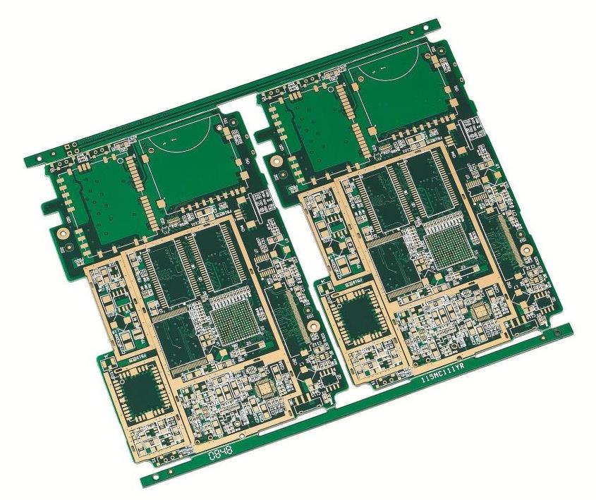
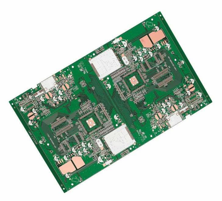
As miniaturization of design has become a fashion, consumers need high-performance, low-priced products. In order to adapt to market competition, manufacturers require R&D personnel to develop high-performance and low-cost products of different types and functional configurations in the shortest possible time. products, occupy the market. This brings many new design challenges to designers. For example, using digital-analog hybrid technology or even radio frequency technology on the same substrate to achieve the purpose of miniaturizing design and improving product function. The mobile phone that took the world by storm is a typical example. The industry also has corresponding solutions - design teams, concurrent design, derivation, and design reuse are typical strategies.
traditional serial design
That is after the electronic engineer completes all the front-end circuit design, it is handed over to the physical board-level designer to complete the back-end implementation. The design cycle is the sum of circuit design and board-level design time. After the novel parallel design of miniaturization became the mainstream design idea and the hybrid technology was widely adopted, the serial design method was somewhat outdated. We must innovate in design methods, and use powerful EDA tools to assist designers in design, in order to meet the requirements of the timely market. As we all know, it is impossible for each of us to be in all fields, and it is impossible to complete all the work quickly in a short period of time. The concept of the design group was proposed in this context and was widely used. Many companies currently take a design team approach to collaborative product development. That is, according to the complexity of the design and the difference of functional modules, the entire design is divided into different functional BLOCK blocks, and different design developers carry out the logic circuit and PCB board design in parallel; then at the top level of the design, the final design results of each BLOCK block, Transfer in the way of "device" to synthesize a whole board design. This approach is called PCB board design reuse. Through this method, it is not difficult to see that it can greatly shorten the design cycle, and the design time is only the sum of the design time of the BLOCK block that takes a lot of time, and the time of the back-end interface connection processing.
Derivative technology
In order to meet the needs of users at different levels, manufacturers that focus on civilian products often need to develop products with different functions and grades to occupy the market. In the past, for product development with different functions, we often used different design processes to implement them separately, that is, using different design data to produce boards with different functions to implement products. The disadvantage is that the cost increases and the design cycle is prolonged, and at the same time, the artificial unreliable factor of the product is increased. Many manufacturers now use derivation technology to solve the above problems, that is, use the same design process data to derive products of different functional series, so as to reduce costs and improve the quality of PCB board.