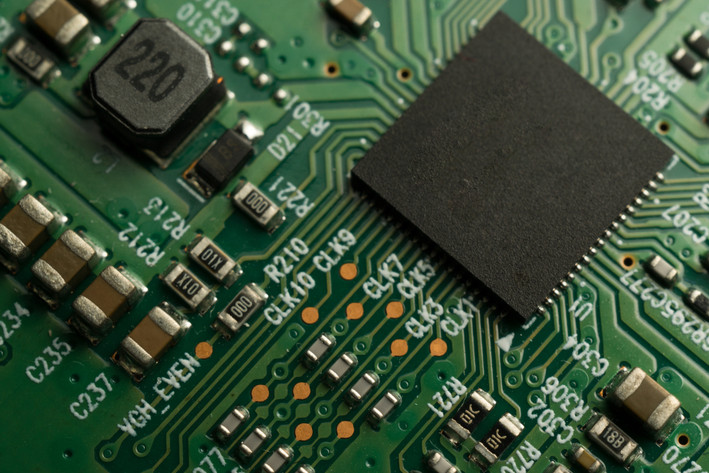
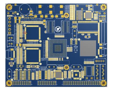
USB is a kind of fast, bidirectional, synchronous transmission, cheap and convenient hot plug serial interface. USB devices are widely used because of their advantages such as fast data transmission, convenient interface, and hot plug support. At present, most of the products on the market use USB2.0 as the interface, but many hardware novices encounter many problems in USB applications. Often, after PCB assembly, USB interfaces have various problems, such as unstable communication or inability to communicate. Check the schematic diagram and welding are all OK. Perhaps it is necessary to suspect that the PCB design is unreasonable at this time. Drawing PCBs that meet USB2.0 data transmission requirements plays an important role in product performance and reliability.
The USB protocol defines that two differential signal lines (D+, D -) transmit digital signals. If the USB device is to work stably, the differential signal lines must be laid and wired in strict accordance with the differential signal rules. Based on the author's years of experience in USB related product design and commissioning, the following points are summarized:

1. During component layout, try to make the differential line as short as possible to shorten the differential line routing distance
2. Give priority to drawing differential lines, and try not to have more than two pairs of vias on one pair of differential lines (vias will increase the parasitic inductance of the line, thus affecting the signal integrity of the line), and place them symmetrically
3. Symmetrical parallel wiring can ensure tight coupling of two wires and avoid 90 ° wiring. Arc or 45 ° wiring is a good way
4. Arrangement of differential series connection resistance capacitance, test point and up and down resistance
5. Due to factors such as pin distribution, vias, and routing space, the differential line length is easy to be mismatched. Once the line length is mismatched, the timing will shift, and common mode interference will be introduced to reduce the signal quality. Therefore, it is necessary to compensate for the mismatch of differential pairs to make the line length match. The length difference is usually controlled within 5mil. The compensation principle is where the length difference is compensated
6. In order to reduce crosstalk, if space allows, the distance between other signal networks and the ground differential line shall be at least 20mil (20mil is an empirical value). If the distance between the ground and the differential line is too close, the impedance of the differential line will be affected
7. The output current of USB is 500mA. Pay attention to the line width of VBUS and GND. If 1Oz copper foil is used, the line width greater than 20mil can meet the current carrying requirements. Of course, the wider the line width, the better the integrity of the power supply.
The line width and line spacing of differential line signal of ordinary USB device should be consistent with that of the whole board. However, when the working speed of the USB device is 480 Mbits/s, it is not enough to do the above. We also need to control the impedance of the differential signal. Controlling the impedance of the differential signal line is very important for the integrity of high-speed digital signals, because differential impedance affects the eye diagram, signal bandwidth, signal jitter and interference voltage of the differential signal line. The differential line impedance is generally controlled at 90 (± 10%) ohms (refer to the chip manual for specific values). The differential line impedance is inversely proportional to the line width W1, W2, T1, the dielectric constant Er1, the line spacing S1, and the distance H1 of the reference layer. The following figure shows the sectional view of the differential line.
The following figure shows the reference stack of the four layer board. The middle two layers are the reference layers. The reference layers are usually GND or Power. The reference layers corresponding to the difference lines must be complete and cannot be divided, otherwise the impedance of the difference lines will be discontinuous. If the four layer board is designed by laminating as shown in Figure 2, the difference line width of 4.5mil and the line spacing of 5.5mil can meet the differential impedance of 90 Ω. However, 4.5mil line width and 5.5mil line spacing are only our theoretical design values. Finally, the circuit board manufacturer will make appropriate adjustments to the line width and line spacing and the distance to the reference layer according to the required impedance value and in combination with the actual production situation and the plate.
The wiring rules described above are based on USB2.0 devices. In the USB wiring process, we should grasp the shortest, tightly coupled, equal length, and consistent impedance of the differential line, and pay attention to the current carrying capacity of the USB power line. It is basically no problem to master the above principles when USB devices operate.