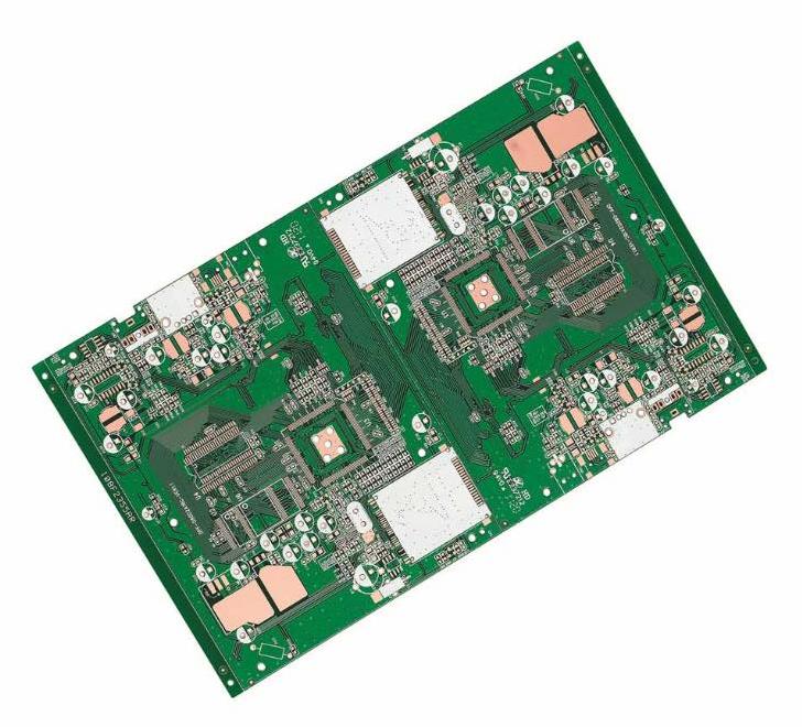
With the wide application of DSP (Digital Signal Processor), the design of a high-speed signal processing PCB board based on DSP is particularly important. In a DSP system, the operating frequency of the DSP microprocessor can be as high as hundreds of MHz, and its reset line, interrupt line and control line, integrated circuit switch, high-precision A/D conversion circuit, and circuits containing weak analog signals are all It is very easy to interfere; so to design and develop a stable and reliable DSP system, anti-interference design is very important. Interference, or interfering energy, puts the receiver in an undesired state. There are two types of interference: direct (coupling via conductors, common impedance, etc.) and indirect (coupling via crosstalk or radiation). Many electrical emission sources, such as light, motors, and fluorescent lamps, can cause interference, and there are three necessary ways for electromagnetic interference (EMI) to have an impact, namely, the interference source, the propagation route, and the interference receptor. It only needs to cut off one of them. Electromagnetic interference problem.

1. Analysis of interference generation in the DSP system
In order to make a stable and reliable DSP system, the interference must be eliminated from all aspects, even if it cannot be completely eliminated, it should be reduced as much as possible. For DSP systems, the main interference comes from the following aspects:
1) Input and output channel interference. It means that the interference enters the system through the forward channel and the backward channel, such as the data acquisition link of the DSP system, and the interference is superimposed on the signal through the sensor, which increases the error of the data acquisition. In the output link, interference can increase the output data error, or even be completely wrong, causing the system to crash. Optocoupler devices can be used reasonably to reduce the interference of input and output channels. For the interference of sensors and DSP main systems, electrical isolation can be used to introduce positive interference.
2) Interference of the power system. The main source of interference for the entire DSP system. When the power supply provides power to the system, it also adds noise to the power supply, so the power line must be decoupled when the power chip circuit is designed.
3) Space radiation coupling interference. Coupling via radiation is often referred to as crosstalk. Crosstalk occurs when electrical current flows through wires, resulting in electromagnetic fields that induce transient currents in adjacent wires, causing adjacent signals to distort or even erroneously. The strength of crosstalk depends on the device, the geometry of the wires, and the separation distance. In DSP wiring, the larger the distance between signal lines and the closer to the ground line, the more effectively the crosstalk can be reduced.
2. Design the PCB board for the cause of the interference
The following gives the method of how to reduce various disturbances in the PCB board fabrication process of the DSP system.
2.1 Laminated design of multilayer boards
In the DSP high-speed digital circuit, in order to improve the signal quality, reduce the difficulty of wiring, and increase the EMC of the system, the stacked design of multi-layer boards is generally used. The stacked design can provide a short return path, reduce the coupling area, and suppress differential mode interference. In a stacked design, dedicated power and ground planes are allocated, and the ground and power planes are tightly coupled to suppress common-mode interference (use adjacent planes to reduce power plane AC impedance). There is a power layer below the top layer, and the power pins of the components can be directly connected to the power supply without passing through the ground plane. The key signals are selected on the bottom layer (bottom layer) so that the important signal routing space is larger, and the devices are placed on the same layer as much as possible. If not necessary, do not make a board with 2-layer parts, which will increase assembly time and assembly complexity. Such as the top layer, only when the top layer components are too dense, devices with limited height and low heat generation, such as decoupling capacitors (patches), are placed on the bottom layer. For the DSP system, there may be a large number of wires to be laid, and the stacked design can be used to route the wires on the inner layer. If traditional through holes waste a lot of valuable routing space, blind buried vias can be used to increase the routing area.
2.2 Layout Design
In order to obtain the performance of the DSP system, the layout of the components is very important. First place DSP, Flash, SRAM, and CPLD devices, which should carefully consider the routing space, and then place other ICs according to the principle of functional independence, and consider the placement of I/O ports. Consider the size of the PCB board in combination with the above layout: if the size is too large, the printed lines will be too long, the impedance will increase, the anti-noise ability will decrease, and the cost of making the board will also increase; if the PCB board is too small, the heat dissipation will be poor, and Space is limited and adjacent lines are easily disturbed. Therefore, the device should be selected according to the actual needs, and the size of the PCB should be roughly calculated based on the wiring space. When laying out the DSP system, special attention should be paid to the placement of the following components.
1) High-speed signal layout: In the entire DSP system, the main high-speed digital signal lines are between DSP, Flash, and SRAM, so the distance between the devices should be as close as possible, and the connections should be as short as possible and directly connected. Therefore, in order to reduce the impact of transmission lines on signal quality, high-speed signal traces should be as short as possible. It is also necessary to consider that many DSP chips with a speed of several hundreds of MHz require snake-like winding. This will be highlighted in the wiring below.
2) Digital-analog device layout: Most of the DSP systems are not single functional circuits, and a large number of digital devices and digital-analog hybrid devices of CM0S are used, so the digital/analog devices should be laid out separately. The analog signal devices should be concentrated as much as possible so that the analog ground can draw an independent area belonging to the analog signal in the middle of the entire digital ground, so as to avoid the interference of the digital signal with the analog signal. Some digital-analog hybrid devices, such as D/A converters, it is traditionally regarded as an analog device, and it is placed on the analog ground, and a digital loop is provided to them so that the digital noise is fed back to the signal source to reduce the digital noise. Effects on the analog ground.
3) The layout of the clock: For the clock, chip select, and bus signals, it should be kept away from the I/O lines and connectors as far as possible. The clock input of the DSP system is easily disturbed, and its processing is very critical. Always keep the clock generator as close as possible to the DSP chip and keep the clock lines as short as possible. The case of the clock crystal oscillator is grounded.
4) Decoupling layout: In order to reduce the instantaneous overshoot of the voltage on the power supply of the integrated circuit chip, a decoupling capacitor is added to the integrated circuit chip, which can effectively remove the influence of the burr on the power supply and reduce the power loop on the PCB board. reflection. Adding a decoupling capacitor can bypass the high-frequency noise of the integrated circuit device, and can also be used as a storage capacitor to provide and absorb the charging and discharging energy at the moment of switching the gate of the integrated circuit. In the DSP system, decoupling capacitors are placed on each integrated circuit, such as DSP, SRAM, Flash, etc., and are added between each power supply and the ground of the chip, and special attention should be paid to decoupling capacitors as close as possible to the power supply end and IC. part foot. Ensure the purity of the current from the power supply end (source end) and into the IC, and minimize the noise path as much as possible. When dealing with capacitors, use large vias or multiple vias, and the connection between vias and capacitors should be as short and thick as possible. When the two vias are far apart, the path is too large, which is not good; the more closely the two vias of the decoupling capacitor are, the better, so that the noise can reach the ground with a short path. In addition, it is very beneficial to add high-frequency capacitors at the power input or where the battery is powered. Under normal circumstances, the value of the decoupling capacitor is not very strict. Generally, it is calculated according to C=l/, that is, when the frequency is 10 MHz, a capacitor of 0.1 μF is taken.
5) The layout of the power supply: When developing the DSP system, the power supply needs to be carefully considered. Because some power chips generate a lot of heat, they should be prioritized in a location that is conducive to heat dissipation and should be separated from other components by a certain distance. Heat dissipation can be performed by adding heat sinks or placing copper under the device. Be careful not to place heating components on the bottom layer of the development board.
6) Other notices: For the layout of other components of the DSP system, the requirements for ease of welding, ease of debugging, and aesthetics should be considered as much as possible. For example, adjustable devices such as potentiometers, adjustable inductance coils, variable capacitors, and DIP switches should be placed in combination with the overall structure. For devices exceeding 15 g, a fixed bracket should be added and then welded, and special attention should be paid to the positioning hole of the PCB board and the position occupied by the fixed bracket. The distance between the components on the edge of the PCB board and the edge of the PCB board is generally not less than 2 mm, the PCB board is rectangular, and the aspect ratio is 3:2 or 4;3.
2.3 Wiring Design
After comprehensively considering the increase of the anti-interference of the DSP system and the enhancement of the EMC capability for layout, some measures and skills must be used in the wiring.
1) DSP wiring: The wiring generally starts from the device and expands around it. For devices packaged in PQFP (Plastic Quad FIat Pack) or BGA (BaIl Grid Array) such as DSP, the routing direction should be roughly determined according to the layout position of SRAM, Flash, and CPLD, and the pins should be fan-out. Fan-out is especially important for QFP&BGA-type devices. At the beginning of wiring, fan-out the pins of BGA-type devices can save time for subsequent wiring and improve the quality and efficiency of wiring. When routing, rationally use the features of EDA tools, such as dynamic routing of power PCB boards, to plan space. When using dynamic, this function will automatically keep the space between lines within the rules, without wasting space, reducing subsequent modifications, and improving the quality and efficiency of wiring. For high-speed DSP, also pay attention to crosstalk and delay tune routing processing. Snaking line processing can ensure the integrity of the signal and the continuity of the reference plane of the high-speed signal. When it is necessary to divide the plane, be careful not to let the high-speed line cross the discontinuous plane; if it must be crossed, add the capacitor across the plane. When the signal line (trace) is spaced three times the signal line width, the probability of mutual crosstalk (coupling) between the signals is only about 25%, so the anti-electromagnetic interference (EMI) requirements can be met. Therefore, for high-speed signal lines such as CLK and SRAM, remember to stay away from the signal line next to it by more than 3 times the width. When the length is adjusted, that is, the serpentine trace, the width of the line and the line should be more than 3 times the width of the signal line, including For its own signal line, it is also three times as wide as the signal line. The line width is 5 mil, and the distance inside the winding itself is 15 mil, which is greater than or equal to 3 times the line width.
2) Clock wiring: For the clock signal, make the wiring distance for other signals as large as possible, ensure a distance of more than 4 times the line width, and do not route under the clock (part); for analog voltage input lines, the reference voltage terminal and the I/O signal line are as far away from the clock as possible.
3) Handling of system power: Power is an important part of the system. A separate power supply layer is allocated in the stacking design of the PCB board, but since a DSP system has a variety of digital and analog devices, there are also a variety of power supplies used, so the power supply layer is divided to make devices with the same power supply characteristics. Divided in the same area, it can be connected to the power plane nearby. However, special attention should be paid to making the signal of the reference power plane continuous when dividing. It has been proved by experiments that the current that can pass through the line width of 40 mils can be guaranteed to be 1 A; for the over-hole L, the current of 1 A can pass through the drill diameter of 16 mils, so for the DSP system, the power line can be larger than 20 mil. . For electromagnetic radiation protection on the power line, pay attention to the following points: use bypass capacitors to limit the leakage of AC current on the circuit board; connect a common mode choke coil in series on the power line to suppress the common mode current flowing through the line; wiring close to reducing the magnetic radiation area.
4) Handling of grounding: In all EMC problems, the main problem is caused by improper grounding. The quality of ground wire processing directly affects the stability and reliability of the system. Grounding has the following functions: reducing the common-mode voltage VCM on the output line; reducing susceptibility to static electricity (ESD); reducing electromagnetic radiation. The ground loops of high-frequency digital circuits and low-frequency analog circuits cannot be mixed, and the digital/analog ground must be separated, because when the digital circuit is switched between high and low potentials, the noise will be generated in the power supply and ground; if the ground plane is not separated, the analog signal will still be ground noise. interference. Therefore, multi-point series grounding should be used for high-frequency signals, and the ground wire should be thickened and shortened as much as possible so that in addition to reducing the voltage drop, it is more important to reduce the coupling noise. But for a system, no matter how it is divided, there is only one final ground, but the discharge path is different. Therefore, the digital ground and the analog ground are connected together through magnetic beads or 0 n resistors to eliminate the interference of mixed signals. When dividing the ground plane, the continuity of the reference plane must be guaranteed. For PCB boards with digital/analog coexistence, if the analog signal line is far away, try to make the reference return path also analog ground. This means that an analog ground should be cut along the path of the analog signal in the ground layer to make it refer to the analog ground to ensure the continuity of its reference plane.
5) Other precautions: During wiring, the corners of the wires should generally not be formed into 90° folded lines to reduce the external emission coupling of high-frequency signals. When laying copper on the PCB, try to avoid using a large area of copper foil, otherwise, the copper foil will easily fall off after being heated for a long time; when a large area of copper foil must be used, it can be replaced by a grid, which is conducive to eliminating the copper foil and the substrate. The adhesive is heated to generate volatile gas. The copper foil laid on the penetrating part feet (DIPPIN) is also treated with thermal pads; virtual soldering should be avoided to improve the yield. The input and output sidelines should be avoided to be adjacent to each other to avoid reflection interference; if necessary, add ground wire for isolation. The wiring of two adjacent layers should be perpendicular to each other, and it is easy to generate coupling in parallel. For I/O, different areas of the respective reference planes can be divided, so that different I/O signals will not interfere with each other on the PCB board.