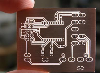
Generally, the layout and wiring rules of PCB board must be understood by everyone. However, do you all know the design rules of the RF board PCB board? Today, let's talk about the layout and wiring principles of the RF board PCB board.
RF board PCB board layout principle
1) Layout determination: Before the layout, you should have a detailed understanding of the board function, working frequency band, current and voltage, main RF device types, EMC, and related RF indicators, and clarify the stack structure, impedance control, external structure size, shielding cavity and cover. The size and position of the device, the processing instructions for special devices (such as the size and position of the device that needs to be hollowed out and directly dissipated by the chassis), etc. In addition, the main RF device power, heat dissipation, gain, isolation, sensitivity and other indicators, as well as the connection of filtering, biasing, and matching circuits, should also be specified. For the power amplifier circuit, the matching routing requirements recommended in the device manual or the RF field analysis software simulation Obtained impedance matching circuit guidelines.
2) Physical partition: The key is to arrange the main components according to the flow direction of the main signal of the single board. First, fix the components on the RF path according to the position of the RF port, and adjust their orientation to reduce the length of the RF path to . In addition to the general layout rules, it is also necessary to consider how to reduce the mutual interference and anti-interference ability of each part to ensure sufficient isolation of multiple circuits. For circuit modules with insufficient isolation or sensitive and strong radiation sources, consider using The metal shield shields the RF energy from the RF area.
3) Electrical partition: The layout is generally divided into three parts: power supply, digital and analog, which must be separated in space, and the layout and wiring cannot cross areas. And try to separate the strong and weak current signals, separate the digital and analog, and the circuits that complete the same function should be arranged within a certain range as much as possible, thereby reducing the signal loop area.

RF board PCB board wiring principle
1) Keep digital circuits away from analog circuits as much as possible, ensure that the RF traces refer to a large-area ground plane, and run the RF traces on the surface as much as possible.
2) The digital and analog signal lines are not routed across regions. If the RF wiring must pass through the signal line, it is preferable to route a ground connected to the main ground along the RF wiring between them; the second option is to ensure that the RF wiring is connected to the main ground. Cross the signal line to reduce capacitive coupling, and at the same time put as much ground as possible around each RF trace and connect to the main ground. In general, the RF printed lines should not be wired in parallel and should not be too long. If parallel wiring is really needed, a ground wire should be added between the two wires (the ground wire should be drilled through holes to ensure good grounding). RF differential line, run parallel lines, add ground lines outside the two parallel lines (ground lines are drilled through holes to ensure good grounding), and the characteristic impedance of the printed lines is designed according to the requirements of the device.
3) The basic sequence of RF printed circuit board wiring: RF line → baseband RF interface line (IQ line) → clock line → power supply part → digital baseband part → ground.
4) Considering that green oil will have an impact on the performance and signal of the microstrip line, it is recommended that the microstrip line with high frequency can not be coated with green oil, and the single board microstrip line with medium and low frequency is recommended to be coated with green oil. .
5) The RF traces are usually not punched. If the RF traces must be changed, the size of the vias should be reduced to , which not only reduces the path inductance, but also reduces the chance of RF energy leaking to other areas in the laminate.
6) Duplexers, IF amplifiers, and mixers always have multiple RF/IF signals that interfere with each other. The RF and IF traces should be crossed as much as possible, and a ground should be spaced between them.
7) Except for special purposes, it is forbidden to protrude excess wire ends on the RF signal traces.
8) The wiring of the baseband RF interface line (IQ line) should be wider, more than 10mil, in order to avoid phase error, the line length should be as equal as possible, and the spacing should be as equal as possible.
9) The RF control line requires the wiring to be as short as possible, and the wiring length is adjusted according to the input and output impedance of the transmission control signal device to reduce the introduction of noise. Keep traces away from RF signals, non-metallized vias, and "ground" edges. Do not drill ground vias around the traces to prevent signals from being coupled to the RF ground through the vias.
10) Keep digital wiring and power wiring away from RF circuits as much as possible; clock circuits and high-frequency circuits are the main sources of interference and radiation, and must be arranged separately and away from sensitive circuits.
11) The main clock wiring is required to be as short as possible, the line width is recommended to be more than 10mil, and the two sides of the trace are grounded to prevent interference from other signal lines. It is recommended to use stripline routing.
12) The control line of the voltage-controlled oscillator (VCO) must be kept away from the RF signal, and the VCO control line can be subjected to packet processing if necessary on PCB board.