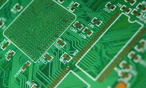
PCB board copying is also often referred to as circuit board copying, circuit board cloning, circuit board copying, PCB cloning, PCB reverse design or PCB reverse research and development in the industry. That is, on the premise of existing electronic products and circuit boards, reverse analysis of circuit boards is carried out by means of reverse R&D technology, and the PCB board documents and bill of materials (BOM) documents of the original products are translated
Parts, schematic documents and other technical documents as well as PCB screen printing production documents shall be restored 1:1. Then use these technical documents and production documents for PCB manufacturing, component welding, flying probe testing, PCB debugging, and complete the copy of the original PCB template.

Many people don't know what PCB copying is. Some people even think that PCB copying is a copycat. In our understanding, copycat means imitation, but PCB copying is not imitation. The purpose of PCB copying is to learn foreign electronic circuit design technology, then absorb the design scheme, and then use it to develop and design more products. With the continuous development and deepening of the board reading industry, today's concept of PCB board reading has been extended to a wider range. It is no longer limited to the copying and cloning of simple circuit boards, but also involves the secondary development of products and the research and development of new products. For example, through the analysis of existing product technical documents, design ideas, structural characteristics, process technology, etc., we can provide feasibility analysis and competitive reference for the R&D and design of new products, assist the R&D and design unit to follow up the technology development trend, adjust and improve the product design scheme in time, and develop new products with market competitiveness. Through the extraction and partial modification of the technical documents, the PCB board copying process can realize the rapid updating, upgrading and secondary development of various types of electronic products. According to the document drawing and schematic diagram extracted from the copied board, the designer can also optimize the design and modify the PCB according to the wishes of the customer. On this basis, new functions can also be added to the product or the functional features can be redesigned, so that products with new functions will appear at a fast speed and in a new attitude, not only with their own intellectual property rights, but also win in the market, it is the first opportunity to bring double benefits to customers. Whether it is used to analyze PCB principle and product working characteristics in reverse research or used as PCB design basis and basis in forward design, PCB schematic diagram plays a special role. Then, how to reverse the schematic diagram of the PCB according to the document diagram or physical object, and what is the reverse process. What kind? What details should I pay attention to?
1. Reverse thrust steps
1) Record PCB related details
After getting a PCB, first record the models, parameters, and positions of all components on the paper, especially the directions of diodes, transistors, and IC notches. Take two photos of component positions with a digital camera. A lot of PCB boards are getting bigger and bigger. The diode triode on the top is not noticeable.
2) Scanned image
Remove all components and remove the tin from the PAD hole. Clean the PCB board with alcohol, and then put it into the scanner. When the scanner scans, it needs to slightly raise some scanning pixels to get a clearer image. Then polish the top layer and bottom layer slightly with gauze until the copper film is bright, put it into the scanner, start PHOTOSHOP, and use color method to
The two layers are swept in respectively. Note that PCB boards must be placed horizontally and vertically in the scanner, otherwise the scanned image cannot be used.
3) Adjust correction image
Adjust the contrast and lightness of the canvas to make the part with copper film contrast strongly with the part without copper film, and then turn the secondary image to black and white to check whether the lines are clear. If not, repeat this step. If it is clear, save the picture as black and white BMP format files TOP BMP and BOT BMP. If you find a problem with the picture, you can also use PHOTOSHOP to repair it
And amendments.
4) Verify the position coincidence of PAD and VIA
Convert the two BMP format files into Protel format files, and transfer them into two layers in Protel. If the positions of pad and via passing through the two layers basically coincide, it indicates that the previous steps are well done. If there is any deviation, repeat step 3. Therefore, PCB copying is a very patient work, because a small problem will affect the quality and the matching after copying
Degree.
5) Paint Layer
Convert the BMP of the TOP layer to the TOP PCB. Note that it should be converted to the SILK layer, which is the yellow layer. Then you can trace lines on the TOP layer and place components according to the drawings in the second step. Delete SILK layer after drawing. Repeat until all layers are drawn.
6) Combined drawing of TOP PCB and BOT PCB
In PROTEL, call in the TOP PCB and the BOT PCB, and it is OK to combine them into a picture.
7) Laser printing TOP LAYER, BOTTOM LAYER
Use the laser printer to print TOP LAYER and BOTTOM LAYER on the transparent film (1:1 scale), put the film on the PCB, and compare whether there is any error. If it is correct, you will be finished.
8) Testing
Test whether the electronic technical performance of the board is the same as that of the original board. If it is the same, it is really finished.
2. Pay attention to details
1) Reasonably divide functional areas
When reverse designing the schematic diagram of a good PCB, reasonable division of functional areas can help engineers reduce some unnecessary trouble and improve the efficiency of drawing. In general, components with the same function on a PCB board will be arranged in a centralized manner, so that functional division can provide convenient and accurate basis for reversing schematic diagrams. However, the
Division is not arbitrary. It requires engineers to have a certain understanding of electronic circuit related knowledge. First, find out the components in a functional unit, and then find out other components of the same functional unit according to the routing connection to form a functional partition. The formation of functional partition is the basis of schematic drawing. In addition, in this process, don't forget the ingenuity
Using the serial numbers of components on the circuit board, they can help you partition functions faster.
2) Alignment reference piece
This reference piece can also be said to be the main component PCB network used at the beginning of schematic drawing. After the reference pieces are determined, they are drawn according to the pins of these reference pieces, which can ensure the accuracy of schematic drawing to a greater extent. For engineers, the determination of benchmark is not very complicated. Generally, they can choose to play a major role in the circuit
As reference pieces, the components and parts of are generally large in size, with many pins, which are convenient for drawing, such as integrated circuits, transformers, transistors, etc., and can be used as appropriate reference pieces.
3) Correctly distinguish lines and reasonably plot wiring
For the distinction of ground wire, power wire and signal wire, engineers also need to have relevant knowledge of power supply, circuit connection, PCB wiring, etc. The distinction of these circuits can be analyzed from the connection of components, the width of circuit copper foil and the characteristics of electronic products. In wiring drawing, to avoid line crossing and interpenetration, a large number of ground wires can be used
With the grounding symbol, different lines of different colors can be used for various lines to ensure clear identification. Special marks can also be used for various components, and even unit circuits can be drawn separately and combined.
4) Master the basic framework and learn from similar schematic diagrams
For the frame composition and schematic drawing method of some basic electronic circuits, engineers need to be proficient. They should not only be able to directly draw the basic composition form of some simple and classic unit circuits, but also be able to form the overall frame of electronic circuits. On the other hand, do not neglect that the same type of electronic products have certain similarities in schematic diagrams
Based on the accumulation of experience, teachers can fully learn from similar circuit diagrams to reverse the new product schematic diagram.
5) Check and optimize
After the schematic diagram is drawn, the reverse design of the PCB schematic diagram can be said to be completed only after the testing and verification. The nominal values of components sensitive to PCB distribution parameters need to be checked and optimized. According to the PCB board file diagram, the schematic diagram needs to be compared, analyzed and checked to ensure that it is completely consistent with the file diagram.