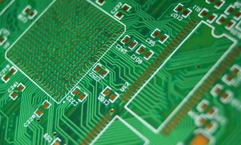
For the PCB board, SMT chip reflow soldering technology requires that the pads of two end Chip components should be independent pads. When the bonding pad is connected with a large area of ground wire, cross paving method and 45 ° paving method shall be preferred; The length of the lead wire from the large area ground wire or power line is more than 0.5mm and the width is less than 0.4mm; The wire connected to the rectangular pad shall be led out from the center of the long side of the pad to avoid a certain angle.

What are the precautions for the direction and shape of the printed wire of PCB pad, and the direction and shape of the printed wire
1) The printed wire of the circuit board in the SMT should be very short. Therefore, if it can be short, it should not be complicated. It should be easy to follow, not complicated, and not long. It is very helpful for the quality control of PCB in the later stage.
2) The direction of the printed wire shall not have sharp bending and acute angle, and the angle of the printed wire shall not be less than 90 °. This is because it is difficult to corrode small internal corners when making plates. The copper foil is easy to peel or warp at the outer corners that are too sharp. The form of turning is gentle transition, that is, the inside and outside corners of the corner are radians.
3) When the wire passes between two gaskets but is not connected with them, it shall be kept at an equal distance from them; Similarly, the distance between conductors shall be uniform and equal and maintained.
4) When connecting wires between PCB pads, when the center distance between pads is less than the outer diameter D of pads, the width of wires can be the same as the diameter of pads; When the center distance between pads is greater than D, the wire width shall be reduced. When there are more than 3 pads on the pad, the distance between wires should be greater than 2D.
5) Copper foil shall be reserved for common grounding wire as far as possible.
6) In order to increase the peeling strength of the gasket, a production line without conductive effect can be provided on the PCB board.