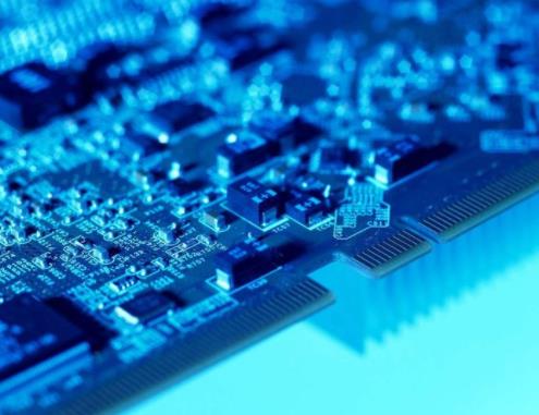
RF microwave circuit PCB is used for various products based on wireless technology. If you are developing robots, smartphones, security applications or sensors, you need to select the perfect RF microwave PCB for your product. With the progress of technology, new designs and products are entering the market every day. These advances have brought about major changes in electronic products. For product developers, what they are very interested in is finding the right PCB for their products to ensure smooth operation and long life. Looking for the perfect RF microwave PCB may have pressure on your project, especially when selecting the right PCB material. For project developers, it is of great interest that their PCBs may be advanced materials with appropriate functions and should be delivered in time. When RF and other parameters are used to select perfect materials for PCB materials, microwave energy level, operating frequency, operating temperature range, current and voltage requirements are very important.

When you begin to manufacture a PCB board, make sure that you have selected a specification that is appropriate for your PCB. The traditional high-frequency RF microwave frequency is a single layer PCB built on the dielectric. However, with the development of RF microwave PCB design, many technologies have emerged in the past decades. Modern PCB combines various digital and mixed signal technologies, so layout and design become more challenging, especially when RF and microwave are mixed for sub components. Whether you are cooperating with us, or with other RF PCB suppliers, or designing your own RF PCB, you need to consider some matters. First, the RF frequency range is typically 500 MHz to 2 GHz, but designs above 100 MHz are often considered RF PCBs. If you risk more than 2 GHz, you are in the microwave frequency range. RF and microwave PCB designs have some major differences - differences between them and your standard digital or analog circuits. Simply put, RF PCB is using analog signals that are essentially very high frequency. Your RF signal can be at almost any voltage and current level at any point in time, as long as it is between your minimum and maximum limits. RF and microwave PCB transmit signals at one frequency and within a certain frequency band. A band-pass filter is used to transmit a signal in a "frequency band of interest" and to filter any signal outside the frequency range. The frequency band can be narrow or wide, and can be transmitted through high-frequency carriers.
High frequency PCB and PCB design principles are as follows:
1) Distributed parameter circuit is not only reflected in the transformation from centralized parameter to distributed parameter, but also more importantly, the signal processing and transmission of PCB circuit begin to partially follow the inherent characteristics of electromagnetic wave. The higher the operating frequency, the more prominent this characteristic is.
2) The concept of reflected wave is the fundamental concept to improve the output power or efficiency of the circuit, otherwise it will lead to a series of problems inconsistent with the design.
3) The investigation of distributed parameters involves some basic physical definitions in electromagnetic wave theory. It is one of the fundamental means to solve the design practice to carefully grasp the embodiment and calculation method of these physical definitions in the circuit.
4) The distribution parameter characteristics of the PCB strip assembly line of microwave grade high-frequency circuit can be characterized by the expression embodied by some relationship constants, and the PCB design purpose can be achieved through these constants.
PCB design principles involve many aspects, including basic principles, anti-interference, electromagnetic compatibility, safety protection, etc. For these aspects, especially in high-frequency circuits (especially microwave level high-frequency circuits), the lack of relevant concepts often leads to the failure of the entire R&D project. Many people still stay on the basis of "connecting electrical principles with conductors to play a predetermined role", and even believe that "PCB design belongs to the consideration of structure, process and improving production efficiency". Many professional RF engineers did not fully realize that this link should be the special focus of the entire design work in RF design, and they mistakenly spent their energy on selecting high-performance components, resulting in a substantial increase in cost and negligible improvement in performance. In particular, it should be pointed out that digital circuits rely on their strong anti-interference, error detection and correction, and can arbitrarily construct various intelligent links to ensure the normal function of the circuit. A common digital application circuit with high additional configuration of various "normal" links is obviously a measure without product concept. However, the links that are often considered "unworthy" lead to a series of product problems. The reason is that such functional links, which are not worthy of reliability assurance from the perspective of product engineering, should be based on the working mechanism of the digital circuit itself. They are just misconstrued in circuit design (including PCB design), resulting in an unstable state of the circuit. The problem caused by this unstable state, which is similar to the problem of high-frequency PCB, belongs to the basic application under the same concept.