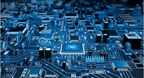
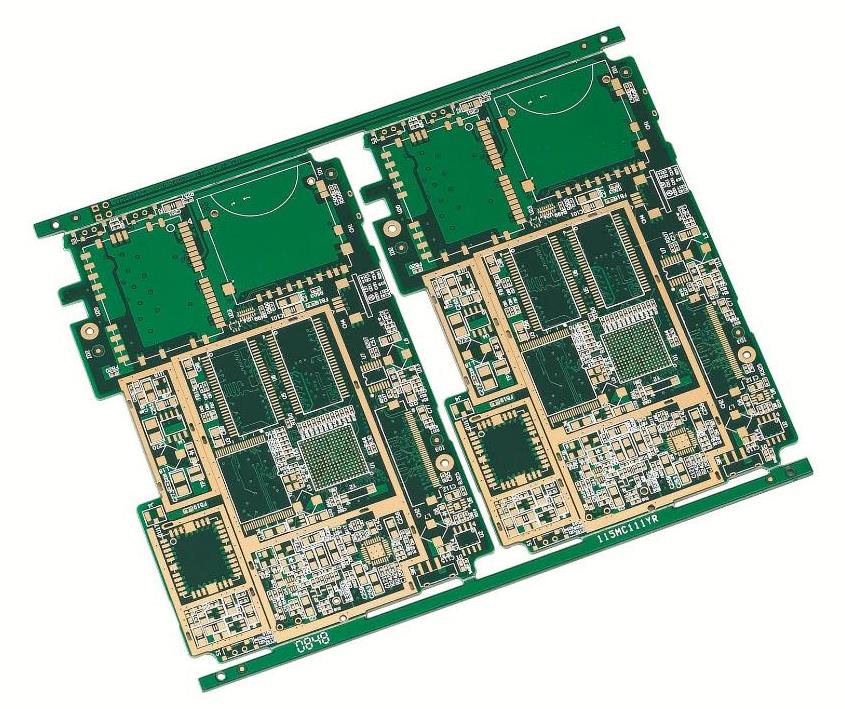
HDI PCB is a circuit board designed to maximize the density of surface components and provide breakthrough solutions and/or transmit high-frequency signals for ICs with a large number of closely spaced pins or pads. The aim is to provide greater functionality in smaller packages. To achieve this goal, you need to select a contract manufacturer (CM) that has the equipment and expertise required to achieve the specialization required for HDI PCB electronic manufacturing. In order to optimize the manufacturing of pcb design, you should follow a clear path or design techniques, which should combine your design intent with the functionality of CM.
Design Skills of HDI PCB Electronic Manufacturing
PCB layout design can be very complex, so designers are required to make difficult decisions about assigning the most important specifications. If the design is aimed at key system industries, such as aerospace, medical equipment, automobile or automobile manufacturing, the process will be more complex. Military, or to obtain high-performance Internet of Things (IoT) or HDI. Regardless of the type of pcb design, when designers combine the benefits of manufacturing design (DFM) for PCB development and coordinate with its CM functions.
DFM is not generic. This is a set of rules and guidelines for specific manufacturing phases, such as design for assembly (DFA) and design for testability (DFT). DFM can also focus on specific board design types, such as HDI. Let's look at some important design techniques aimed at optimizing the manufacturing of HDI PCB electronic products.

Tip 1: Select a through-hole type to minimize process complexity
The selection of through-hole is a crucial decision, which not only determines the required equipment and manufacturing steps, but also affects processing time and additional costs. The use of blind or buried micropores helps to reduce the number of layers and material costs; However, whether to use the dog bone shaped or near pad via in the selected pad will affect the complexity of the process.
Tip 2: Select the minimum number of components to apply HDI
The choice of components is always important. However, component selection optimization is more important for HDI boards. HDI designed the components to determine the width, location, type and size of drilling and stacking. Obviously, performance is the primary consideration, but packaging, traceability and availability should also be considered. The need to replace components or redesign the layout can increase additional manufacturing time and material costs.
Tip 3: Space components minimize stress and EMI
When the components are placed so that the through-hole positions are asymmetrically distributed, uneven stresses may be applied to the plate, which may lead to warping. This will seriously affect the yield and the number of boards available for each panel. If the components are separated from the dense high power components, the signal may introduce electromagnetic interference (EMI) in the track, thus affecting the signal quality. In addition, parasitic capacitance and/or inductance of nearby pins or pads may affect signal quality. Therefore, it is recommended to include EMI modeling during design to extract parasitic effects.
Tip 4: Route to minimize signal integrity problems
One of the advantages of HDI is the ability to use a smaller routing width for signal propagation. Although the routing width is reduced, it should be designed to achieve the best width signal integrity. This includes using the shortest routing length, consistent path impedance, adequate ground plane, and digital, analog, and power signal isolation.
Tip 5: Select stacking to minimize material costs
In addition to the selection of through-hole, the selection of PCB stack also has a significant impact on the manufacturing cost of HDI PCB electronic products. The material type and number of layers directly affect the required number of laminations and drilling cycles. In making these decisions, cost should be one of the determining factors.
Following the above tips on HDI PCB electronics manufacturing will help your CM make the process as efficient as possible. However, HDI PCB are not manufactured once and for all. To learn how to integrate design and manufacturing, see the following DFM for HDI case study.