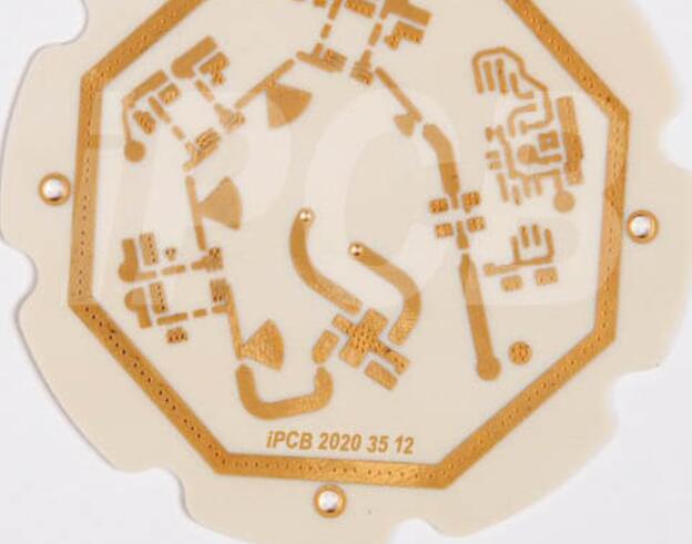
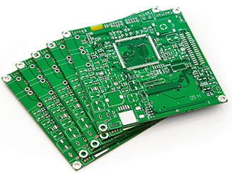
Pcb multilayer board is a special kind of printed circuit board, and its place of existence is generally special, for example, there will be pcb multilayer board in the circuit board.This kind of pcb multilayer board can help the machine to conduct various circuits, not only that, but also can play an insulating role, so that electricity will not collide with each other, and it is absolutely safe.If you want to use a pcb multilayer board with good performance, you must carefully design it. Next, we will explain how to design pcb multilayer boards.
Pcb multilayer board design
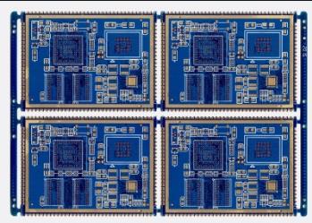
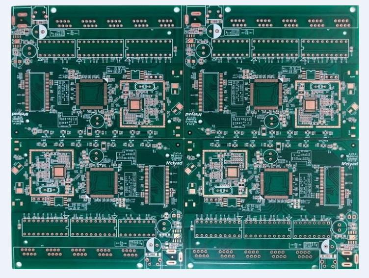
1. Determination of board shape, size and number of layers
1) Any printed board has the problem of matching with other structural parts. Therefore, the shape and size of the printed board must be based on the overall structure of the product. However, from the perspective of production technology, it should be as simple as possible. Generally, it is a rectangle with a small ratio of length to width, which is conducive to improving production efficiency and reducing labor costs.
2) The number of layers must be determined according to the requirements of circuit performance, board size and circuit density. For multilayer printed boards, four layer boards and six layer boards are the most widely used. For example, four layer boards are two wire layers (component surface and welding surface), one power layer and one layer.
3) Each layer of the multilayer board shall be symmetrical, and it is better to have an even number of copper layers, that is, four, six, eight layers, etc. Because of the asymmetric lamination, the board surface is prone to warp, especially for surface mounted multilayer boards, which should be paid more attention.
2. Position and placement direction of components
1) The location and placement direction of components should first be considered from the circuit principle to meet the trend of the circuit. Whether the placement is reasonable or not will directly affect the performance of the printed circuit board, especially the high-frequency analog circuit, which has more stringent requirements on the location and placement of devices.
2) The reasonable placement of components, in a sense, has indicated the success of the PCB design. Therefore, when preparing the layout of printed boards and deciding the overall layout, the circuit principle should be analyzed in detail, and the location of special components (such as large-scale IC, high-power tubes, signal sources, etc.) should be determined first, and then other components should be arranged to avoid possible interference factors.
3) On the other hand, it should be considered from the overall structure of the printed board to avoid uneven arrangement of components. This not only affects the aesthetics of printed boards, but also brings a lot of inconvenience to assembly and maintenance.
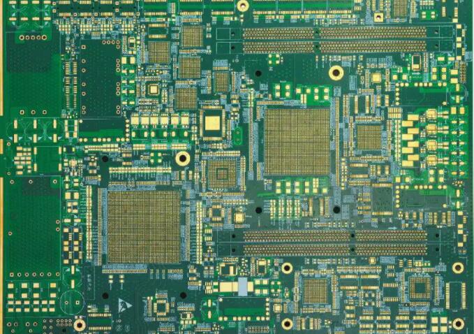
3. Requirements for wire layout and wiring area
In general, the wiring of multilayer printed boards is carried out according to the circuit functions. When wiring in the outer layer, more wiring is required on the welding surface and less wiring is required on the component surface, which is conducive to the maintenance and troubleshooting of printed boards. Thin, dense wires and signal wires susceptible to interference are usually arranged in the inner layer.
Large area copper foil should be evenly distributed in the inner and outer layers, which will help to reduce the warpage of the plate and also enable a more uniform coating on the surface during electroplating. In order to prevent the appearance processing from damaging the printed wire and causing interlayer short circuit during machining, the distance between the conductive pattern in the inner and outer wiring areas and the board edge shall be greater than 50mil.

4. Requirements for wire direction and width
The power supply layer, stratum and signal layer shall be separated for multi-layer board wiring to reduce the interference between power supply, ground and signal. The lines of two adjacent layers of printed boards shall be as perpendicular to each other as possible or take oblique lines and curves instead of parallel lines to reduce the interlayer coupling and interference of the substrate.
And the wire should be short as far as possible. Especially for small signal circuits, the shorter the wire, the smaller the resistance and the smaller the interference. For signal lines on the same layer, sharp corners shall be avoided when changing direction. The width of the conductor shall be determined according to the current and impedance requirements of the circuit. The power input line shall be larger and the signal line may be smaller.
For general digital boards, the line width of power input line can be 50~80mil, and that of signal line can be 6~10mil.
Conductor width: 0.5, 1, 0, 1.5, 2.0;
Allowable current: 0.8, 2.0, 2.5, 1.9;
Conductor resistance: 0.7, 0.41, 0.31, 0.25;
During wiring, the width of lines shall be as consistent as possible to avoid sudden thickening and thinning of wires, which is conducive to impedance matching.
5. Requirements for drilling size and pad
1) The size of the drill hole for components on the multilayer board is related to the pin size of the selected components. If the drill hole is too small, the assembly and tin of the components will be affected; The drilling is too large, and the welding spot is not full enough during welding. In general, the calculation method of element hole diameter and pad size is:
2) Hole diameter of element hole=element pin diameter (or diagonal)+(10~30mil)
3) Element pad diameter ≥ element hole diameter+18mil
4) As for the hole diameter, it is mainly determined by the thickness of the finished board. For high-density multilayer boards, it should generally be controlled within the range of plate thickness: hole diameter ≤ 5:1. The calculation method of via pad is:
5) Diameter of via pad (VIAPAD) ≥ via diameter+12mil.
6. Requirements for power layer, stratum partition and trepanning
For multilayer printed boards, there is at least one power supply layer and one stratum. Since all the voltages on the printed board are connected to the same power layer, the power layer must be isolated by zones. The size of the zone line is generally 20~80 mil wide. The higher the voltage, the thicker the zone line.
For the connection between the welding hole and the power layer and the stratum, in order to increase its reliability and reduce the false welding caused by the large area of metal heat absorption during the welding process, the general connection plate shall be designed in the form of a flower hole. Hole diameter of isolation pad ≥ hole diameter+20mil.
7. Requirements for safe spacing
The setting of safety distance shall meet the requirements of electrical safety. In general, the minimum distance between outer conductors shall not be less than 4mil, and the minimum distance between inner conductors shall not be less than 4mil. If the wiring can be arranged, the spacing should be as large as possible to improve the yield of the finished board and reduce the hidden trouble of the finished board.
8. Requirements for improving the anti-interference capability of the whole board
In the design of multilayer printed boards, attention must also be paid to the anti-interference ability of the whole board. The general methods are:
a. Add a filter capacitor near the power supply and ground of each IC, and the capacity is generally 473 or 104.
b. For the sensitive signals on the printed board, the accompanying shielded wires shall be added separately, and the wiring near the signal source shall be minimized.
c. Select a reasonable grounding point.
Have you understood all the above pcb multilayer board skills? In the face of today's rapid development of electronic equipment, pcb design is faced with these trends of high performance, high speed, high density, light and thin. PCB design of high-speed signal has increasingly become the focus and difficulty of electronic hardware development, which pays more attention to efficiency and rigor.
In such a big environment, as an Allegro engineer, if you can skillfully use the powerful functions of Cadence Allegro, your works will play a full role in high-speed design! Teacher Fan Yi PCB Huang teaches you to deal with it around!
In order to solve the current situation of pcb multilayer board, Fanyi Education launched this crowdfunding course. Starting from the fundamental skills of pcb multilayer board, it adopted the method of "breaking things up": dividing products into PCB modules, then elaborately explaining the key points of PCB layout and wiring of each module, and then integrating them into different products, so as to fundamentally solve the limitations of pcb multilayer board product thinking. No matter what PCB design they do after learning, In fact, it is to integrate the key points of the layout and wiring of each module, 80% of the workload of a board is completed, and the remaining 20% is the interconnection between modules and the copper filling of power supply, which can be quickly grasped through our full set of procedural PCB video practical skills!