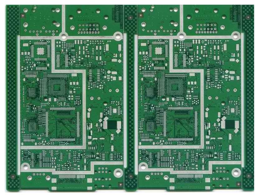
In electronic equipment, printed circuit board is a key part. It carries other electronic parts and connects circuits to provide a stable working environment for circuits. So, what are the PCB proofing processes? Take the six ply board as an example to understand:

1) PCB board inner line: the copper foil substrate shall be cut into the size suitable for processing and production. Before pressing the film on the substrate, it is usually necessary to roughen the copper foil on the plate surface properly, and then attach the dry film photoresist to it with appropriate temperature and pressure; Then, the substrate is sent to the ultraviolet exposure machine for exposure, and the line image on the negative is transferred to the dry film photoresist on the board surface. After tearing off the protective adhesive film, first develop and remove the area without light on the film surface with sodium carbonate aqueous solution, and then remove the exposed copper foil with hydrogen peroxide mixed solution to form a circuit. Finally, the dry film was washed off with light sodium oxide aqueous solution.
2) Pressing: Before pressing, the inner laminates are blackened (oxygenated) to passivate the copper surface and increase insulation; The copper surface of the inner circuit is roughened to produce good adhesion. When overlapping, rivet the inner PCB with more than six layers of lines (including) with rivet machine; Then put them neatly between the mirror steel plates in a container and send them to the vacuum press to harden and bond the film with appropriate temperature and pressure. The pressed circuit board takes the target hole drilled by the X-ray automatic positioning drilling machine as the reference hole; The plate edge shall be cut properly to facilitate subsequent processing.
3) Drilling: use CNC drilling machine to drill out the conductive holes of the circuit between layers and the fixing holes of the welding parts.
4) Plated through-hole: after forming the interlayer conductive through-hole, a metal copper layer shall be laid on it to complete the conduction of the interlayer circuit. First, clean the burr on the hole and the dust in the hole by heavy brushing and high pressure washing, and soak and attach tin on the clean hole wall.
5) Primary copper: the circuit board is immersed in the chemical copper solution, and the copper ions in the solution are reduced and deposited on the hole wall to form a through hole circuit; Then, the copper layer in the through hole is thickened by copper sulfate bath electroplating to the thickness enough for subsequent processing.
6) Secondary copper of outer circuit: The production of circuit transfer is similar to that of inner circuit, but the circuit etching is divided into two ways: positive and negative. The negative film is made in the same way as the inner circuit. After development, it is directly etched with copper and removed from the film. The way of positive film is to add secondary copper and tin lead plating after development. After removing the film, the exposed copper foil is corroded and removed with a mixed solution of ammonia and copper chloride to form a circuit; Finally, remove the tin lead layer with tin lead stripping solution.
7) Solder proof ink text printing: the text, trademark or part number required by the customer is printed on the board by screen printing, and then the text paint ink is hardened by heating (or ultraviolet radiation).
8) Contact processing: the soldering proof green paint covers most of the copper surface of the circuit, and only the terminal contacts for parts welding, electrical testing and circuit board plugging are exposed. The end point shall be additionally provided with a proper protective layer to avoid the generation of oxides during long-term use, which may affect the stability of the circuit.
9) Forming and cutting: cut the circuit board into the external dimensions required by customers with CNC forming machine; Finally, clean the powder on the circuit board and the ionic pollutants on the surface.
10) Inspection board packaging: common packaging PE film packaging, heat shrinkable film packaging, vacuum packaging, etc.
In the production process of PCB aluminum substrate, in order to ensure its good application effect, the tin wire is usually welded manually afterwards. Then, what problems should be paid attention to when soldering the PCB aluminum substrate manually?
1) Pay attention to welding temperature
Due to the particularity of aluminum substrate materials, in order to ensure the welding effect, it is necessary to ensure the operation of the temperature level during welding. The welding temperature should be kept as constant as possible, and the welding accuracy should be paid attention to. Only in this way can the very good application effect be guaranteed.
2) Select suitable raw materials
In the welding process, it is particularly important to select the appropriate raw materials. Try to select some ultra-low temperature electrodes and their relative welding fluid, so that the welding effect will be better.
3) It is harmful to apply force to spot welding with soldering iron
The soldering iron head transfers the heat to the spot welding. The key is to increase the total contact area. The use of electric soldering iron for spot welding has no effect on heating. In many cases, it can cause damage to the welded parts. Soldering points such as resistors, power switches, and connectors are usually fixed on plastic prefabricated components. The result of force application is likely to lead to invalid components. Although manual welding is rarely used for mass production and manufacturing of electronic equipment, manual welding is still unavoidable for the maintenance and adjustment of electronic equipment. At the same time, as a highly theoretical professional skill, the quality of PCB board welding will also damage the maintenance effect.