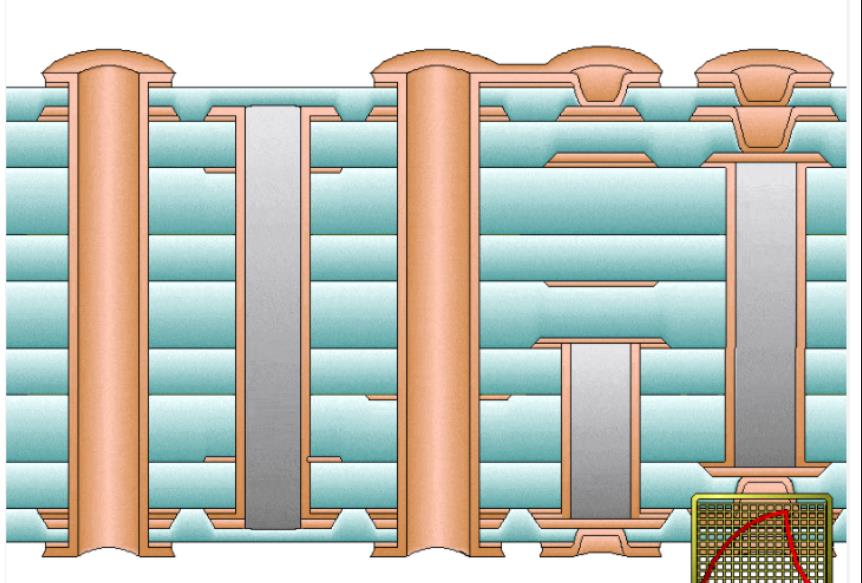
For the incomplete solder joint in BGA repair in FR-4 PCB, it means that the volume of the solder joint is insufficient, and the BGA solder joint with reliable connection cannot be formed in BGA welding. The characteristic of the incomplete solder joint is that the shape of the solder joint is obviously smaller than other solder joints during AXI inspection. For this BGA problem, the root cause is insufficient solder paste. Another common cause of incomplete solder joints encountered in BGA repair is the cored phenomenon of solder. BGA solder flows into the through-hole due to capillary effect to form information. Chip offset or tin offset, as well as the absence of solder mask separation between the BGA pad and the defected vias, may lead to wicking, resulting in the underfilled BGA solder joint. It should be noted that if the solder mask is damaged during the repair of BGA devices, it will aggravate the occurrence of wicking phenomenon, resulting in the formation of incomplete solder joints. Incorrect design will also lead to the formation of incomplete solder joints. If the hole in the BGA pad is designed, a large part of the solder will flow into the hole. At this time, if the amount of solder paste provided is insufficient, a low Standoff solder joint will be formed. The remedy is to increase the amount of solder paste printing. When designing the steel mesh, the amount of solder paste absorbed by the hole in the plate should be taken into account. The sufficient amount of solder paste should be ensured by increasing the thickness of the steel mesh or increasing the size of the steel mesh opening; Another solution is to use microporous technology to replace the hole design in the plate, so as to reduce the loss of solder.

Another factor that causes incomplete solder joints is the poor coplanarity of devices and PCB. If the solder paste printing quantity is sufficient. However, the gap between BGA and FR-4 PCBis inconsistent, that is, poor coplanarity will also lead to incomplete solder joints. This is particularly common in CBGA. Therefore, the measures to solve the insufficient solder joints in BGA welding mainly include the following:
1) Print enough solder paste;
2) Cover the vias with resistance welding to avoid solder loss;
3) Avoid damaging the solder mask during BGA repair;
4) Accurate alignment of sound when printing solder paste;
5) BGA mounting accuracy;
6) Correct operation of BGA components in the repair stage;
7) Meet the coplanarity requirements of PCB and BGA to avoid warping, for example, appropriate preheating can be taken in the repair stage;
8) The microporous technology is used to replace the hole design in the plate to reduce the loss of solder.
Common problems and welding defects of wave soldering
1) Pull tip
Causes: improper transmission speed, low preheating temperature, low tin pot temperature, small PCB transmission angle, poor wave crest, solder failure, poor solderability of component leads.
Solution: adjust the transmission speed to the appropriate position, adjust the preheating temperature, adjust the temperature of the tin pot, adjust the angle of the conveyor belt, optimize the nozzle, adjust the waveform, change the flux, and solve the solderability of the lead.
2) Bridging
Causes: low preheating temperature, low tin pot temperature, high solder copper content, flux failure or density imbalance, improper PCB layout and PCB deformation.
Solution: adjust the preheating temperature, adjust the tin pot temperature, test the Sn and impurity content of solder, adjust the flux density, or change the flux, change the PCB design, and check the PCB quality.
3) Faulty soldering
Causes: poor solderability of component leads, low preheating temperature, solder problem, low flux activity, too large pad hole, oxidation of printed board, contamination of board surface, too fast conveyor belt speed, low tin pot temperature.
Solution: Solve the solderability of the lead, adjust the preheating temperature, test the content of Sn and impurities in the solder, adjust the flux density, design to reduce the pad hole, remove PCB oxide, clean the board surface, adjust the transmission speed, and adjust the temperature of the tin pot.
4) Tin thin
Causes: poor solderability of component leads, too large pad, too large pad hole, too large welding angle, too fast transmission speed, high temperature of tin pot, uneven application of sweat agent, and insufficient tin content of solder.
Solution: Solve the solderability of the lead wire, design and reduce the solder pad, reduce the welding angle, adjust the transmission speed, adjust the temperature of the tin pot, check the pre-coating flux device, and test the Sn content of the solder.
5) Missing welding (partial welding and opening)
Causes: poor solderability of lead wire, unstable solder wave, invalid flux, uneven flux spraying, poor local solderability of PCB, jitter of transmission chain, incompatibility of precoated flux and flux, and unreasonable process flow.
Solution: Solve the lead solderability, check the wave crest device, replace the flux, check the pre-coating flux device, solve the PCB solderability, check and adjust the transmission device, uniformly use the flux, and adjust the process flow.
6) Large deformation of printed board
Causes: fixture failure, fixture operation problem, uneven pcb pre-heating, high preheating temperature, high tin pot temperature, slow transmission speed, PCB material selection problem, PCB storage moisture, PCB too wide.
7) Poor wettability
Causes: poor solderability of components/pads, poor flux activity, and insufficient preheating/tin pot temperature.
Solution: test the solderability of components/pads, change the flux, and increase the preheating/tin pot temperature in FR-4 PCB.