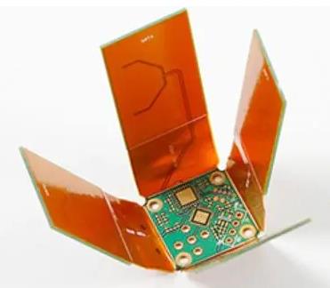
Printed circuit board (PCB) is one of the important components of electronic products. Due to the use of printed circuit boards, errors in wiring and assembly are reduced, equipment maintenance, debugging, and inspection time is saved, and equipment replacement is facilitated. High wiring density, small size, and light weight are conducive to miniaturization of electronic equipment, mechanized, and automated production, improving labor productivity, and reducing the cost of electronic equipment.

ultra thin pcb
In recent years, the trend of circuit boards towards lightweight, thin, small, and high-density interconnections has led to the loading of more micro devices on limited surfaces, which has led to the development of printed circuit board designs towards high-density, high-precision, multi-layer, and small aperture. In order to meet the development requirements of electronic products refinement, electronic products continue to develop in a thinner direction. The thinner and thinner products have brought significant adjustments to the production process of printed circuit boards, and the research and development of new equipment and new processes has been put on the agenda. The purpose is to overcome the shortcomings of the prior art and provide a manufacturing method for fabricating ultra thin PCBs with a thickness of each layer less than 0.05 mm using multilayer copper foils, which can overcome the problems of air leakage pollution caused by the separation of the carrier plate and the copper foil during the processing process of the prior art and the inability to fabricate inner buried holes.
A method for producing ultra thin pcb, the method comprising the following steps:
(1) Select a double-sided copper clad laminate bearing plate 22 with a thickness greater than 0.1 mm to form a positioning pattern 21 on the upper and lower outer surfaces;
(2) After stacking the outer layer copper foil 26, pressing material 23, multi-layer copper foil 27, pressing material 23, carrier plate 22, pressing material 23, multi-layer copper foil 27, pressing material 23, and outer layer copper foil 26 from top to bottom, hot pressing is performed using German Burklemode1lamv100 to produce the required pressing plate, wherein the copper foil and pressing material form an inner layer processing plate;
(3) Perform edge salvage treatment on the pressed plate using an edge salvage machine, and cut the plate with the required size;
(4) Mechanically drilling positioning holes and making through holes for the cut ultra thin pcb;
(5) Conduct circuit fabrication on the required pressing plate, add electroplating processes as needed, and form conductive circuit patterns 210 on the outer copper foil of one or both outer surfaces of the required pressing plate;
(6) Laminate the completed pressing plate to form a new insulating medium layer and conductive layer, and add laser drilling, electroplating, pattern transfer, and other processes as needed;
(7) Repeat step 6 until at least two layers (such as four layers) of multi-layer inner layer processing board 28 with a total thickness greater than 0.08 mm are produced as required;
(8) After trimming the above finished plate, separate the multi-layer copper foil to form the redundant plate 211 and the required multi-layer inner layer processing plate 28;
(9) Conduct graphic transfer production on the upper and lower sides of the multi-layer inner layer processing board. When making each layer, make a graphic transfer before adding layers to make the next layer;
(10) Laminate the two conductive line patterns of the multi-layer inner layer processing board to form a new insulating dielectric layer and conductive layer, and add laser drilling, electroplating, graphics, and other processes as needed;
(11) Repeat Step 10 until the outer layer is processed, and add processes such as mechanical drilling, electroplating insulation protection layer, and surface oxidation protection layer fabrication as needed in ultra thin pcb.