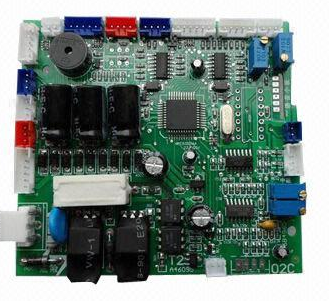
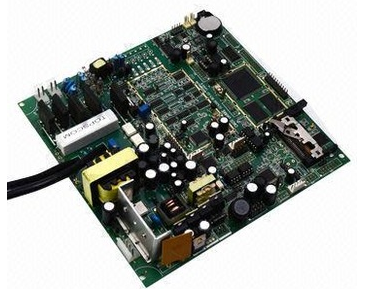
How to avoid defects in SMT patch processing and welding
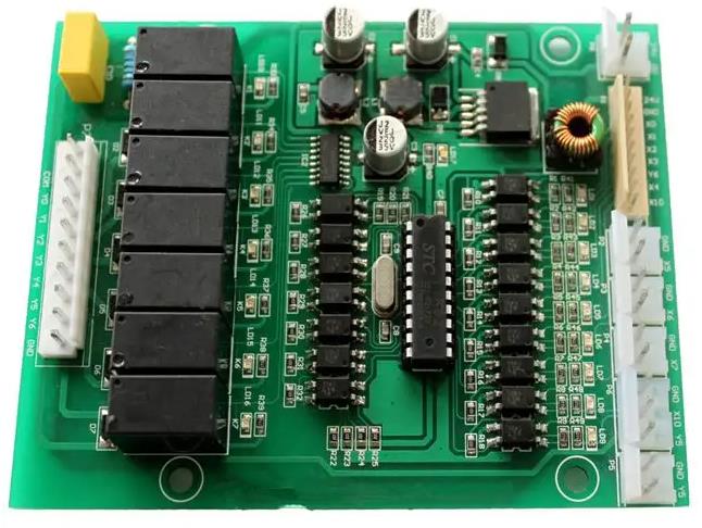
Welding is the most important link in smt patch processing. If the welding link is not done well, it will affect the entire production of the PCB board. If it is a little bit, substandard products will appear, and if it is serious, the product will be scrapped. In order to avoid the impact on the quality of smt processing due to poor welding, it is necessary to pay attention to welding.
For this reason, we have summarized the following seven factors that will affect welding. I hope everyone can help after reading them.

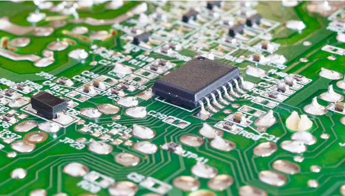
1, welding heating bridge. The soldering thermal bridge in the PCB patch processing is to prevent the solder from forming a bridge. If there is an error in this process, it will cause the uneven distribution of the solder. The correct soldering method is to put the soldering iron tip between the pins of the soldering pad and bring the soldering wire close to the soldering iron tip. When the solder paste melts, move the soldering wire between the soldering pad and the pins, and place the soldering iron on the soldering wire. In this way, good solder joints can be produced and the impact on processing can be reduced.
2. The pins are welded hard. In the process of processing, excessive force in the soldering of the pins can easily lead to problems such as tilting, delamination or depression of the pads of the patch. Therefore, in order to ensure the quality of the smt patch processing during the soldering process, it is not necessary to use too much force, only the soldering iron head needs to be in contact with the pad.
3, the choice of soldering iron tip. In the soldering process, the size of the soldering iron tip is also very important. If the size is too small, the retention time of the soldering iron tip will increase, leading to the appearance of cold solder joints. Excessive size will cause the heating to be too fast and burn to the patch. Therefore, we need to choose the size suitable for the soldering iron tip according to the length and shape of the soldering iron tip, as well as the heat capacity and contact surface.
4, temperature setting. Temperature is also a very important step in the soldering process. Too high a temperature setting will cause the pad to tilt, and excessive heating of the solder will damage the patch. Therefore, it is necessary to pay attention to the temperature setting. Setting a suitable temperature is also particularly important for processing quality.
5. The use of flux. During the implementation of related processes, if the flux is used too much, it will cause the problem of whether the lower solder foot is stable, and if it is serious, corrosion or electron transfer may occur.
6, transfer welding operation. Transfer soldering refers to putting the solder on the tip of the soldering iron first, and then transferring to the connection. The improper operation will cause poor wetting. Therefore, we should first place the soldering iron tip between the pad and the pin. When the soldering iron wire is close to the soldering iron tip, move the soldering wire to the opposite side while waiting for the tin to melt. Then place the tin wire between the pad and the pin. Place the soldering iron on the tin wire and move the tin wire to the opposite side when the tin melts.
7, modification or rework. The biggest taboo in the connection process is to retouch or rework in pursuit of perfection. And this approach is not only indispensable to repeated modification or rework in pursuit of perfect product quality, which is easy to cause the circuit board/PCB circuit board metal layer to break.
There is also board delamination, which not only consumes time but may also cause a scrap of the PCBA board, so do not make unnecessary modifications and rework.