SMT chip processing BGA is a packaging method, BGA is the abbreviation of English BallGridArray, translated as ball grid array packaging. With the continuous development of electronic technology in the 1990s, IC processing speed has also continued to increase. With the continuous increase in the number of I/O pins on the integrated PCB circuit board chip, various levels of factors have clearly raised the importance of IC packaging. These regulations, in addition, in order to consider the development of electronic equipment towards miniaturization and precision, BGA packaging has come out and capital is put into production. The technical professional SMT chip processing factory below briefly introduces the basic processing information of BGA to everyone.
1. Steel mesh
In the specific SMT processing, the thickness of the steel mesh is generally, but the thick steel mesh in the welding process of BGA devices is likely to cause tin connection. According to Pate’s high-precision surface assembly production work experience, the thickness of the steel mesh is for It is very suitable for BGA devices, and it can also moderately expand the total area of the stencil opening.
Two, solder paste
The pin spacing of BGA devices is small, so the used solder paste also stipulates that the metal material particles should be small. Excessive metal material particles will cause the SMT process to appear even tin.
3. Welding temperature setting
In the whole process of SMT patch processing, a reflow oven is generally used. Before soldering BGA package components, the temperature of each area must be set in accordance with the processing regulations and the temperature around the spot welding must be detected by the thermal resistance camera.
4. Inspection after welding
After SMT processing, strict inspections should be carried out on BGA packaged devices to prevent some SMD defects from appearing.
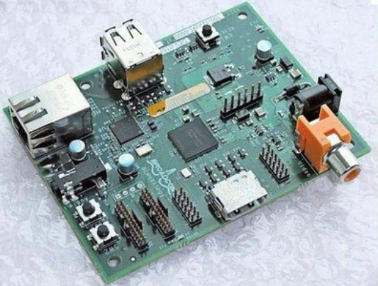
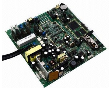
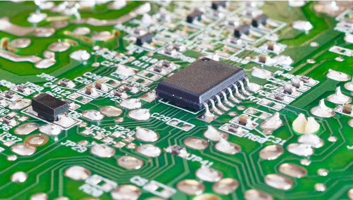
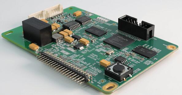
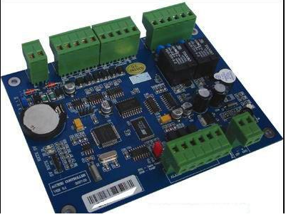
SMT chip processing

Five, the advantages of BGA packaging:
1. Increased assembly yield;
2. Improved electric heating performance;
3. Reduced volume and mass;
4. The parasitic parameters are reduced;
5. The signal transmission delay is small;
6. Increase in frequency of use;
7. Good product credibility;
6. Defects of BGA package:
1. The inspection after welding must be based on X-ray;
2. Increase in electronic production costs;
3. Increased repair costs;
Because of its packaging characteristics, BGA has a very high degree of difficulty in SMT chip soldering, and casting defects and rework are also more difficult to actually operate, in order to ensure the soldering quality of BGA devices. SMT chip processing plants generally focus on the following levels: Pay attention to the order of processing requirements.