Quick look! PCBA processing quality agreement
In the process of PCBA patch processing, the quality control links are very complicated. Every step of this inspection link is related to the quality of the final product, and the quality of the product is directly related to the reputation, so every link cannot be ignored or ignored. Today we will introduce the content of the PCBA processing quality agreement.
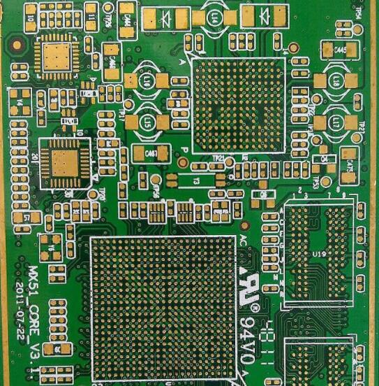
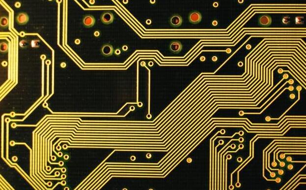
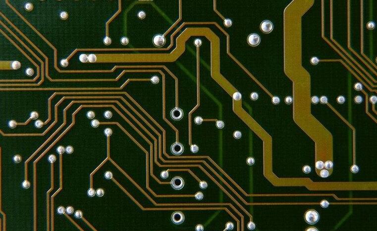
1. PCB circuit board manufacturing
Analyze the Gerber file after receiving the PCBA instruction, pay attention to the relationship between the PCB hole spacing and the board's load-bearing capacity, do not cause bending or breakage, and consider high-frequency signal interference, impedance and other key factors when wiring.
2. Procurement and inspection of components

The procurement of components requires strict control of channels. Excellent PCB manufacturersmust pick up goods from large traders and original factories, and 100% avoid second-hand materials and counterfeit materials. In addition, a special purchase inspection post should be set up to strictly inspect the following items to ensure that the components are free of faults.
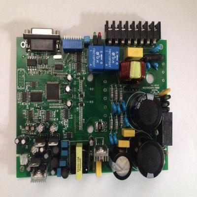
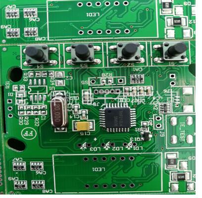
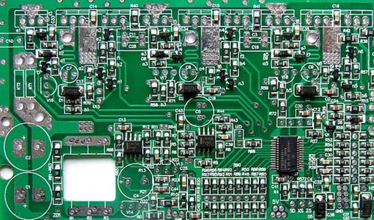
3. SMTAssembly processing
The temperature control of solder paste printing and reflow oven is the key. It is very important to use a laser steel mesh with good quality and meet the process requirements. According to PCB requirements, some steel mesh holes need to be added or reduced, or U-shaped holes are used to make steel mesh according to process requirements. The furnace temperature and speed control of reflow soldering are very important for solder paste infiltration and soldering reliability. It can be controlled according to normal SOP operation guidelines. In addition, AOI testing needs to be strictly implemented to minimize the adverse effects caused by human factors.
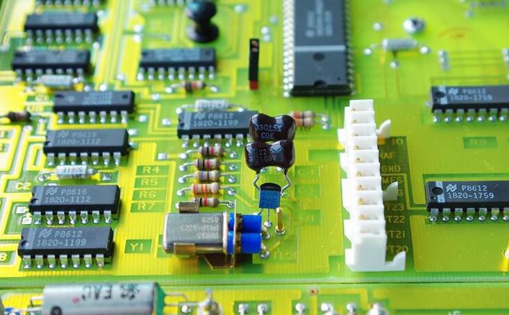
4. DIP plug-in processing
In the plug-in process, the mold design for wave soldering is a key point. How to use molds to maximize the probability of good products after the furnace is a process that PE engineers must continue to practice and summarize experience.
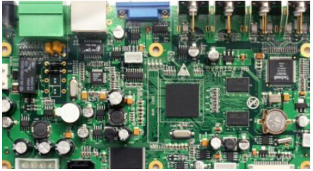
5. Program firing
In the previous DFM report, it is recommended to set some test points on the PCB to test the continuity of the PCB and PCBA circuit after soldering all the components. If possible, you can ask the customer to provide a program, and burn the program into the main control IC through a burner (such as st-link, j-link, etc.) in order to more intuitively test the function changes caused by various touch actions, thereby Test the functional integrity of the entire PCBA.
6. PCBA board test
For orders with PCBA test requirements, the main test content includes ICT (InCircuitTest), FCT (FunctionTest), BurnInTest (aging test), temperature and humidity test, drop test, etc., according to the customer's test plan operation and summary report data that is Can.