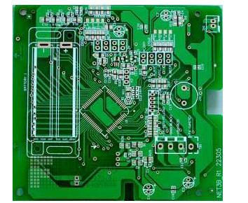
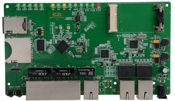
PCBA welding processing requirements for PCB boards
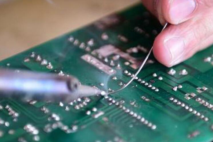
When PCBA welding is processed, there are usually many requirements for PCBA board, and the board must meet the requirements to accept welding processing. So why does the welding process need so many requirements for the board? It turns out that in the process of PCBA processing, there will be a lot of special processes, and the application of special processes immediately brings requirements for the PCB board. If there are problems with the PCB board, it will increase the difficulty of the PCBA soldering process, which may eventually be Lead to welding defects, unqualified boards, etc. Therefore, in order to ensure the smooth completion of the special process and to facilitate the PCBA soldering process, the PCB board must meet the manufacturability requirements in terms of size and pad distance. Then today I will show you how PCBA soldering processing is right. The requirements of the PCB board.

1. PCB size
The width of the PCB (including the edge of the board) should be greater than 50mm and less than 460mm, and the length of the PCB (including the edge of the board) should be greater than 50mm. If the size is too small, it needs to be made into a jigsaw.
2. PCB board edge width
Board edge width: >5mm, panel spacing: <8mm, distance between pad and board edge: >5mm
3. PCB bending
Upward bending degree: <1.2mm, downward bending degree: <0.5mm, PCB distortion: maximum deformation height ÷ diagonal length <0.25
4. PCB board mark point
Mark shape: standard circle, square, triangle;
Mark size: 0.8~1.5mm;
Mark material: gold-plated, tin-plated, copper and platinum;
Mark's surface requirements: the surface is flat, smooth, non-oxidized, and free of dirt;
Mark's surrounding requirements: there should be no green oil or other obstacles within 1mm, which is obviously different from the Mark's color;
Mark position: 3mm above the edge of the board, and there should be no Mark-like vias, test points, etc. within 5mm around the board.
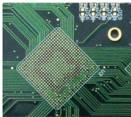
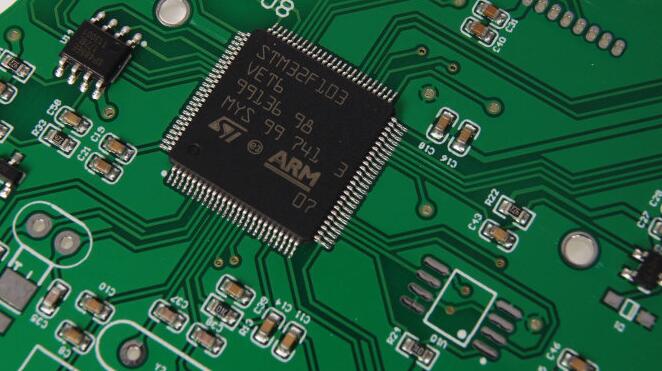
5. PCB pads
There are no through holes on the pads of SMD components. If there is a through hole, the solder paste will flow into the hole, resulting in less tin in the device, or the tin flowing to the other side, causing the board surface to be uneven and the solder paste cannot be printed.
When conducting PCB design and production, it is necessary to understand some knowledge of PCBA welding process, so as to make the product suitable for production. Understanding the requirements of the processing plant first can make the subsequent manufacturing process more smooth and avoid unnecessary troubles.
This is the requirement of PCBA welding processing for PCB boards. When producing PCB boards, do not slacken their efforts. Only by producing high-quality and compliant PCB boards can the board better accept other special processes, and give the PCB board life and inject the soul of function. .