How to choose HASL, ENIG, OSP circuit board surface treatment process?
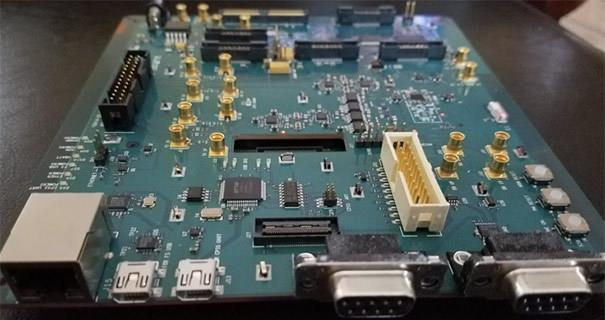
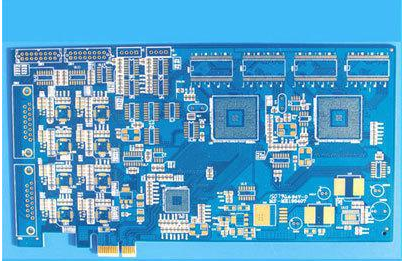
After we design the PCB board, we need to choose the surface treatment process of the circuit board. The commonly used surface treatment processes of the circuit board are HASL (surface tin spraying process), ENIG (immersion gold process), OSP (anti-oxidation process), and the commonly used surface How should we choose the treatment process? Different PCB surface treatment processes have different charges and different final effects. You can choose according to the actual situation. Let me tell you about the advantages and disadvantages of the three different surface treatment processes: HASL, ENIG, and OSP.
1. HASL (Surface tin spraying process)
The tin spray process is divided into lead spray tin and lead-free tin spray. The tin spray process used to be the most important surface treatment process in the 1980s, but now, fewer and fewer circuit boards choose the tin spray process. The reason is that the circuit board is developing in the direction of "small and precise". The tin spraying process will cause the fine components to be soldered with tin beads, and the spherical tin point will cause poor production. PCBA processing plants are pursuing higher process standards and For production quality, ENIG and SOP surface treatment processes are often chosen.
Advantages of lead spray tin: lower price, excellent soldering performance, mechanical strength and gloss are better than lead spray tin.
Disadvantages of lead spray tin: lead spray tin contains lead heavy metals, which is not environmentally friendly in production and cannot pass ROHS and other environmental protection evaluations.

Advantages of lead-free tin spray: low price, excellent soldering performance, and relatively environmentally friendly, and can pass environmental protection evaluations such as ROHS.
Disadvantages of lead-free tin spray: mechanical strength and gloss are not as good as lead-free tin spray.
The common shortcoming of HASL: It is not suitable for welding pins with fine gaps and components that are too small, because the surface flatness of the spray tin plate is poor. In PCBA processing, tin bead is easy to produce, and it is easy to cause short circuit to the fine-gap pin components.
2. ENIG (Immersive Gold Technology)
Immersion gold process is a relatively advanced surface treatment process, which is mainly used on circuit boards with connection functional requirements and a long storage period on the surface.
The advantages of ENIG: It is not easy to oxidize, can be stored for a long time, and the surface is flat. It is suitable for welding small gap pins and components with small solder joints. Reflow soldering can be repeated many times without reducing its solderability. It can be used as a substrate for COB wire bonding.
Disadvantages of ENIG: high cost, poor welding strength, because the electroless nickel process is used, it is easy to have the problem of black disk. The nickel layer will oxidize over time, and long-term reliability is a problem.
3. OSP (anti-oxidation process)
OSP is an organic film formed on the surface of bare copper chemically. This layer of film has anti-oxidation, thermal shock resistance, and moisture resistance to protect the copper surface from rusting (oxidation or vulcanization, etc.) in a normal environment; it is equivalent to an anti-oxidation treatment, but in the subsequent welding high temperature, The protective film must be easily removed by the flux, and the exposed clean copper surface can be immediately combined with the molten solder to form a firm solder joint in a very short time. At present, the proportion of circuit boards using OSP surface treatment process has increased significantly, because this process is suitable for low-tech circuit boards and high-tech circuit boards. If there is no surface connection functional requirement or storage period limitation, the OSP process will be the most ideal The surface treatment process.
Advantages of OSP: It has all the advantages of bare copper welding, and the expired (three months) board can also be resurfaced, but usually only once.
Disadvantages of OSP: easy to be affected by acid and humidity. When used in the secondary reflow soldering, it needs to be completed within a certain period of time, and usually the effect of the second reflow soldering will be relatively poor. If the storage time exceeds three months, it must be resurfaced. It must be used up within 24 hours after opening the package. OSP is an insulating layer, so the test point must be printed with solder paste to remove the original OSP layer before it can contact the pin point for electrical testing. The assembly process needs to undergo major changes. If the unprocessed copper surface is detected, it will be detrimental to ICT. Over-tipped ICT probes may damage the PCB, requiring manual precautions, limiting ICT testing and reducing test repeatability.
The above is about the analysis of the surface treatment process of HASL, ENIG, OSP circuit boards. You can choose which surface treatment process according to the actual use of the circuit board.