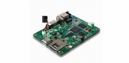
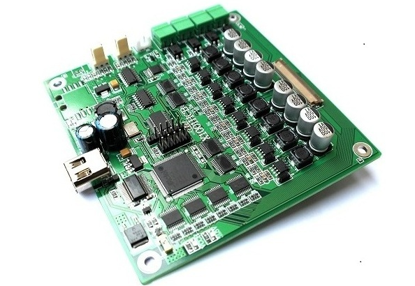
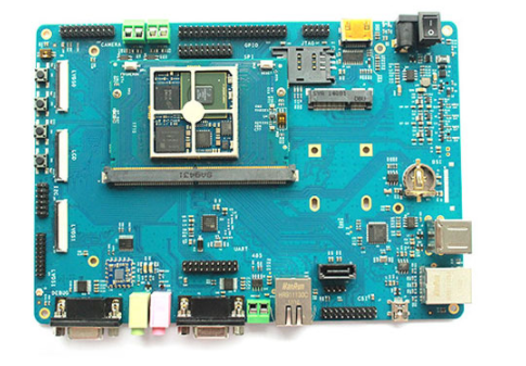
What are the common boarding methods and principles of PCBA circuit boards?
In order to improve production efficiency and reduce production costs in PCBA processing, PCBA circuit boards are usually subjected to imposition production, which can facilitate PCBA processing plants for patch welding. Let's talk about the common imposition methods and principles of PCBA circuit boards.
The principle of PCBA circuit board imposition:
1. The width of the PCB panel is ≤260mm (SIEMENS line) or ≤300mm (the FUJI line); if automatic dispensing is required, the width of the PCB panel is ≤125mm*180mm.
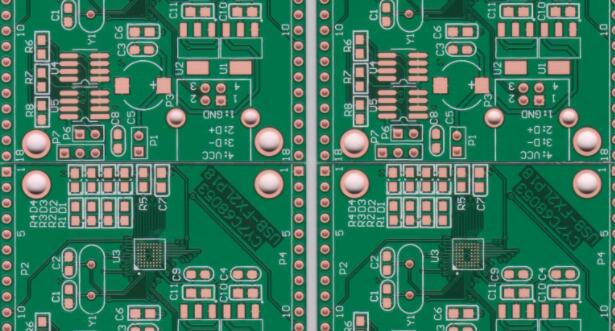
2. The PCB board shape is as close as possible to the square, and 2*2, 3*3, 4*4 and other boards are recommended; but be careful not to build a yin and yang board.
3. The outer frame (clamping side) of the PCB jigsaw should adopt a closed-loop design to ensure that the PCB jigsaw will not be deformed after being fixed on the fixture.

4. The center distance between the small plates is controlled between 75mm and 145mm.
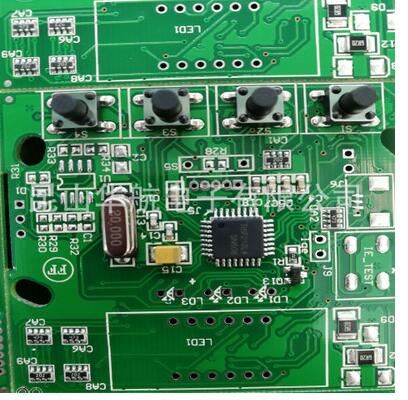
5. There should be no large devices or protruding devices near the connection point between the outer frame of the panel and the inner small board, and between the small board and the small board, and there should be a space greater than 0.5mm between the components and the edge of the PCB board. To ensure the normal operation of the cutting tool.
6. Four positioning holes are made in the four corners of the outer frame of the jigsaw panel, with a diameter of 4mm±0.01mm; the strength of the holes should be moderate to ensure that they will not break during the upper and lower boards; the precision of the hole diameter and position should be high, and the hole wall should be smooth and free of burrs. .
7. Each small board in the PCB jigsaw must have at least three positioning holes, 3≤aperture≤6mm, and no wiring or patching is allowed within 1mm of the edge positioning hole.
8. The reference symbols used for the positioning of the entire PCB and the positioning of fine-pitch devices. In principle, the QFP with a spacing of less than 0.65mm should be set in its diagonal position; the positioning reference symbols used for the imposition PCB sub-board should be paired Used, arranged at the opposite corner of the positioning element.
9. When setting the reference positioning point, usually leave a non-soldering area 1.5mm larger than it around the positioning point.
10. Large components should have positioning posts or positioning holes, such as I/O ports, microphones, battery ports, micro switches, earphone ports, motors, etc.
Common imposition methods for PCBA circuit boards:
1. V-CUT
V-CUT means that several boards or the same board can be combined and spliced together, and then after the PCB processing is completed, a V-cut machine is used to cut a V-shaped groove between the boards, which can be broken during use. It is the more popular way nowadays.
2. Punching
Punching refers to milling out between the board or the inside of the board with a milling machine as needed, which is equivalent to digging out.
3. Stamp hole
The so-called stamp use is to use a small hole to link the board to the board, which looks like the zigzag on the stamp, so it is called the stamp hole link. The stamp hole link requires high control burrs on all four sides between the board and the board, that is, only a small stamp hole can be used to replace the V line.
ipcb is a high-precision and high-quality PCB manufacturer, such as: isola 370hr PCB, high-frequency PCB, high-speed PCB, ic substrate, ic test board, impedance PCB, HDI PCB, Rigid-Flex PCB, buried blind PCB, advanced PCB, microwave PCB, telfon PCB and other ipcb are good at PCB manufacturing.