Talking about the basic principle of smt vacuum reflow soldering
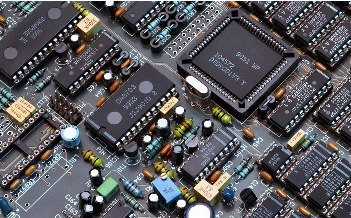
Generally, some cavities will remain in the solder joints of the device after smt patch soldering, which poses a certain potential risk to the reliability of product quality. Although there are many reasons for these voids, such as solder paste,PCBA pad surface treatment, reflow profile settings, reflow environment, pad design, microvias, hollow disks, etc., the main reason is often due to soldering. Caused by residual gas from molten solder. When the molten solder solidifies, these bubbles are frozen to form voids. Voids are a common phenomenon in soldering. It is difficult to have no voids in all solder joints in electronic assembly products. Due to the influence of voids, the quality and reliability of most solder joints are uncertain, resulting in a decrease in the mechanical strength of the solder joints, and will seriously affect the thermal and electrical conductivity of the solder joints, thereby seriously affecting the electrical performance of the device.
In view of this, for the solder joints in the power electronic technology PCB, the void content observed in the X-ray image must not exceed 5% of the overall area of the solder joint. The smallest area ratio of this magnitude cannot be achieved by optimizing existing processes, which means that new soldering processes, such as vacuum reflow oven soldering technology, are required. The vacuum reflow soldering process is a technique for soldering in a vacuum environment. This can fundamentally solve the problem of solder oxidation in a non-vacuum environment during smt patch proofing or processing and production, and due to the pressure difference between the inside and outside of the solder joint, the bubbles in the solder joint can easily overflow from the solder joint. In this way, the bubble rate in the solder joint is very low or even no bubbles, and the expected purpose is achieved.
Vacuum reflow soldering technology provides the possibility of preventing gas from entering the solder joints and forming voids. This is especially important when large-area soldering. Because these large-area solder joints need to conduct high-power electrical and heat energy, the voids in the solder joints are reduced. In order to fundamentally improve the thermal conductivity of the device. Vacuum welding is sometimes mixed with reducing gas and hydrogen to reduce oxidation and remove oxides.

The basic principle of vacuum reflow oven to reduce voids in the soldering process can be analyzed from four aspects:
1. The vacuum reflow furnace can provide a very low oxygen concentration and a suitable reducing atmosphere, so that the oxidation degree of the solder is greatly reduced;
2. Due to the reduction of the oxidation degree of the solder, the gas reacted by the oxide and the flux is greatly reduced, thus reducing the possibility of voids;
3. Vacuum can make the molten solder have better fluidity and lower flow resistance, so that the buoyancy of the bubbles in the molten solder is much greater than the flow resistance of the solder, and the bubbles are very easy to be discharged from the molten solder;
4. Due to the pressure difference between the bubble and the outside vacuum environment, the buoyancy of the bubble will be very large, making the bubble very easy to get rid of the limitation of the molten solder. After vacuum reflow soldering, the bubble reduction rate can reach 99%, the void rate of a single solder joint can be less than 1%, and the void rate of the entire PCB board can be less than 5%. On the one hand, it can increase the reliability and bonding strength of the solder joints, and the wettability of the solder. On the other hand, it can reduce the use of solder paste during use, and it can improve the solder joints to adapt to different environmental requirements, especially high temperatures. Humid, low temperature and high humidity environment.
You can order as little as 1PCB from us. We will not force you to buy things you really don't need to save money.
Free DFM
Before you pay in the most timely manner, all your orders will receive free engineering document review services by our well-trained professional and technical personnel.