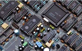
How about the specific process of PCBA processing welding cooling?
In the chip processing industry, everyone knows that soldering is the most important process in the PCB processing production process. But why does the welded product need to undergo a cooling process? How to cool down? What are the temperature limits? Today, let Baiqian be your detailed explanation of PCBA processing welding temperature cooling process.
1. PCB processing welding from peak temperature to freezing point.
In this area is the liquid phase zone, a too slow cooling rate is equivalent to increasing the time above the liquidus line, which will not only increase the thickness of the IMC rapidly, but also affect the formation of the solder joint microstructure, which has a great impact on the quality of the solder joint. A faster cooling rate is beneficial to reduce the formation rate of IMC.

The rapid cooling near the freezing point (between 220 and 200°C) is beneficial to the non-eutectic lead-free solder to reduce the plastic time range during the solidification process. Shortening the time that the PCB assembly board is exposed to high temperatures is also beneficial to reduce the damage to the heat-sensitive components.
In addition, we must also see that rapid cooling will increase the internal stress of the solder joints, which may cause SMT patch solder joint cracks and component cracking. Because during the soldering process, especially during the solidification process of the solder joints, due to the large differences in the coefficient of thermal expansion (CTE) or thermal properties of various materials (different solders, PCB materials, Cu, Ni, Fe-Ni alloys), When the solder joints are solidified, due to the cracking of related materials, welding defects such as cracks in the plating layer in the PCB metallized holes will occur. These situations will occur, and we must do a good job of inspection.
2. From the vicinity of the solidus (solidification point) of the solder alloy to 100°C.
The long time from the solidus of the solder alloy to 100°C will increase the thickness of the IMC on the one hand. On the other hand, for some interfaces with low melting point metal elements, segregation may occur due to the formation of dendrites. It is easy to cause peeling defects of solder joints. In order to avoid the formation of dendrites, the cooling should be accelerated, and the cooling rate from 216 to 100°C is generally controlled at -2 to -4°C/s.
3. From 100°C to the outlet of the reflow soldering furnace.
Considering the protection of operators, the temperature at the outlet is generally required to be lower than 60°C. The outlet temperature of different furnaces is different. For equipment with high cooling rate and long cooling zone, the outlet temperature is lower. In addition, during the aging process of lead-free solder joints, the thickness of the IMC will be slightly increased if the time is too long. In short, we must consider the difference of different materials, we need to set different temperatures to correspond
In short, the cooling rate has a great influence on the quality of PCB processing and welding, which will affect the long-term reliability of electronic products. Therefore, it is very important to have a controlled cooling process.