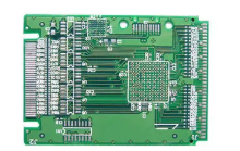
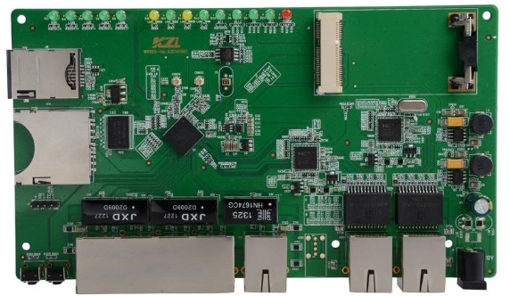
What issues should be paid attention to in the design of PCBA board manufacturability?
When designing PCBA boards, engineers must start from reducing costs and improving assembly quality on the premise of meeting the requirements of the overall mechanical and electrical performance, mechanical structure and reliability. So, what issues should be paid attention to in the design of PCBA board manufacturability? The following Xiaoqiancheng editor will explain to you in detail:
1. Minimize the number of PCB layers. Can use single-sided board instead of double-sided board, and can use double-sided board instead of multi-layer board, so as to reduce PCB processing cost as much as possible.
2. Try to use reflow soldering process, because reflow soldering has more advantages than wave soldering.
3. Minimize the process of PCB assembly process and try to use no-clean process.
4. Whether it meets the requirements of SMT technology and equipment for PCB design.

5. Whether the PCB shape and size are correct, and whether the small-size PCB considers the splicing process.
6. Whether the clamping edge design and positioning hole design are correct.
7. Whether the positioning holes and non-grounding installation holes are marked with non-metallization.
8. Whether the Mark graphic and its position meet the regulations, and whether 1~1.5mm is reserved around it to the solder mask.
9. Whether the requirements of environmental protection have been considered.
10. Whether the selection of substrate materials, components and packaging meet the requirements.
11. Whether the PCB pad structure (shape, size, spacing) meets the DFM specification.
12. Whether the lead width, shape, spacing, and the connection between the lead and the pad meet the requirements.
13. Whether the overall layout of the components and the minimum spacing between components meet the requirements; whether the rework size is considered around the large components, and whether the polarity arrangement direction of the components is as consistent as possible.
14. Whether the aperture and pad design of the plug-in components meet the DFM specification; whether the distance between adjacent plug-in components is conducive to manual plug-in operation.
15. Whether the solder mask and screen graphics are correct, and whether the component polarity and IC pin are marked.
We are not an agent
Our factory is located in China. For decades, Shenzhen has been known as the world's electronics R&D and manufacturing center. Our factory and website are approved by the Chinese government, so you can skip the middleman and buy products on our website with confidence. Because we are a direct factory, this is the reason why 100% of our old customers continue to purchase on iPCB.
No minimum requirements
You can order as little as 1 PCB from us. We will not force you to buy things you really don't need to save money.
Free DFM
Before you pay in the most timely manner, all your orders will receive free engineering document review services by our well-trained professional and technical personnel.