Although AOI equipment originated 20 years ago, for a long period of time, it was expensive and difficult to grasp, and the detection results were not satisfactory. AOI only existed as a concept and was not recognized by the market. However, since 2005, AOI has developed rapidly. AOI equipment suppliers have sprung up like bamboo shoots after rain. Various new concepts and new products have emerged one after another. In particular, AOI equipment manufacturers in China are the pride of our smt industry, and the AOI equipment produced is in use. In effect, it is no longer up and down with foreign products, and because of the rise of AOI production, the overall price of AOI has dropped to 1/2 to 1/3 of the previous one. Therefore, in terms of the labor cost saved by AOI instead of manual visual inspection, buying AOI is also It is worthwhile, not to mention that using AOI can also increase the straight-through rate of the product and obtain a more stable detection effect than manual. So AOI is already a necessary equipment for smt processing manufacturers.

Under normal circumstances, AOI can be placed in 3 positions in the smt production process, after printing the solder paste, before reflow soldering, and after reflow soldering to monitor the quality of different sections. Although the use of AOI has become a trend, most manufacturers still only install AOI behind the furnace, and use AOI as the gatekeeper for the flow of products into the next section, only instead of manual visual inspection. In addition, many manufacturers still have misunderstandings about AOI. No AOI can achieve no false test, and no AOI can achieve no missed test. Most AOIs choose the right balance between false test and missed test, because the algorithm of AOI is either way. Compare the current sample with the computer sample (either an image or a parameter), and make a judgment based on the similarity.
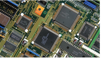
At present, there are still many dead spots in the AOI after the furnace is used. For example, the single-lens AOI can only detect part of the QFP, SOP, and false welding. However, the detection rate of multi-lens AOI for QFP and SOP's lifted feet and less tin is only 30% higher than that of single-lens AOI, but it increases the cost of AOI and the complexity of operating programming. These images are produced using visible light. AOI is powerless to detect invisible solder joints such as BGA missing balls and PLCC false soldering.
After being placed in the solder paste printing, the AOI that detects the quality of the solder paste printing is called SPI by industry insiders. At present, only a few large-scale enterprises or FPCB enterprises are equipped with such equipment. Speed, accuracy, misjudgment rate and price are the reasons that restrict the popularization of this equipment.
At present, the AOI placed in front of the furnace is very rarely used, and it is only used for some products that cannot be detected after the furnace (such as some mobile phone panels with a shielding cover, which must be tested before the shielding cover is installed) or products with poor detection results (such as soft boards) ).
In addition, there is an appearance inspection equipment AXI that has emerged in recent years, which is under rapid development. A number of online AXI devices have appeared in the 2009 NEPCON exhibition. Many testing equipment suppliers are optimistic about the future development of AXI, because AXI can truly solve the blind spot of single-lens AOI detection. The rise of online AXI makes more The AOI of the lens becomes meaningless. AXI uses invisible light Xray to inspect PCB assembly. Its advantages are as follows: Defects that can be inspected include: virtual soldering, bridging, tombstones, insufficient solder, pores, missing components, IC lifted feet, IC less tin, and so on. In particular, X-RAY can also inspect hidden solder joints such as BGA, PLCC, and CSP. Because the image is a binary image, image recognition is relatively easy to complete, with low false positives. Its disadvantages are: slow speed, high price, very few real online use, mostly offline use. At present, online machines are not yet mature and have not been recognized and accepted by PCB manufacturers.