Failure analysis of PCBA
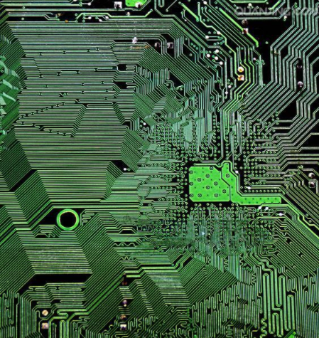
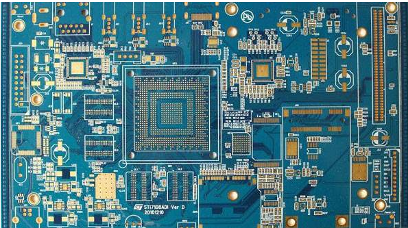
PCBA is a system composed of PCB and various electronic components. The main material of PCB is a composite material of glass fiber and epoxy resin, which is divided into single-sided, double-sided and multi-layer boards.
PCBA failure characteristics
1. Mechanical damage
Due to the stress of bending, twisting, etc., the components may be damaged. For SMD components, the solder joints of some components may be cracked or the components may be damaged. On PCBs with through holes, the package of the components may be cracked, or the pins may fall off the main body of the component.
2. Thermal damage
- Excessive voltage applied to the circuit board causes excessive current, and for smaller circuits or components, their power consumption capacity leads to over-electricity damage (EOS);
- Damage caused by the external heat source of the equipment;
-Thermal damage caused by component failure (long-term high temperature causes epoxy resin to become carbonized and black)

3. Pollution
- The flux is not cleaned;
- leave fingerprints, dust or cleaning fluid during processing;
-metal fragments or solder bridging from assembly;
- Encountered polluted atmosphere during storage, equipment installation or operation;
-Moisture or salt in the environment. Pollutants in the environment can cause corrosion of copper lines and reduce insulation. Pollutants
can cause corrosion of copper circuits. After a long period of time, contaminants may cause metal migration. There are two forms: whisker growth and dendrite growth.
When identifying contaminants, the most commonly used microscope and SEM, EDX, or FTIR, SIMS, XPS and other technologies.
4. Thermal expansion mismatch
When materials with different thermal expansion coefficients are physically connected together, their size changes with temperature, especially when the temperature changes drastically, which can cause mechanical failure.
5. Component interconnection failure on PCB
Interconnection failures mostly occur on solder joints, at the interface between multilayer boards and at the connection of pads. The pores between several layers and the through holes and the cracks in the circuit cause the connection to fail. Contaminants in the solder can also cause weak solder joints, which can cause solder joint cracks. Thermal stress, mechanical stress, and process problems can all cause interconnect failures. In addition, the thermal expansion of volatile organic compounds (VOCs) can cause pores or cracks, which can cause connection failures.
PCB failure analysis steps
1. Visual inspection
Cracks on the substrate indicate the presence of stresses such as bending, and overheated or discolored lines are a sign of overcurrent. Cracked solder joints indicate solderability problems or solder contamination. Some solder joints have dark surfaces or too much or too little solder. These characteristics are signs of poor soldering technology, contamination or overheating. Any discoloration is possible. Means overheating. Solder reflows to create porosity, which means high temperature.
2. X-ray
Check for any disconnection/shorting or circuit damage, incompletely filled through holes, misaligned circuit or component pads.
3. Electrical measurement
is used to confirm cracked and broken solder joints, leakage caused by pollutants, voltage can be applied to measure current, but the voltage should be limited to a reasonable range. Applying some stress during the test may find some intermittent abnormalities.
4. Sectional analysis
For solder joints and internal defects of multilayer boards, the method of preparing metallographic samples can be used to check.
5. SEM and EDX
Contaminants on the surface of the substrate can be identified by SEM. Contaminants may appear on the surface of the board or under the conformal coating. Sometimes the conformal coating must be removed first without affecting the contaminants, chlorine, fluorine, sulfur, and Bromine is an element of concern, and bromine is a flame retardant component that plays a flame retardant effect in certain materials. EDX can be used to check the presence of contaminants in the solder joints. Sulfur, oxygen, copper, aluminum and zinc are all contaminants that may cause problems in the solder joints. The solder joint cracks caused by contaminants often occur at the interface between the component pins and the solder. At the intermetallic compound.
The method of removing the conformal layer:
1. Dissolve with a solvent. Solvents such as xylene, trichloroethane, methyl acetaldehyde, ketone and methylene chloride can remove the conformal layer, but do not damage the board or contaminants.
2. Thermal separation, using a controllable low-temperature heating method. This method is best for thick coatings. Heat is directly applied to the coating to separate it from the base material.
3. Grind off, use a spraying equipment similar to sandblasting to remove those coatings that are impossible to melt away with solvents.
4. Plasma etching, place the board in a vacuum chamber and use low-temperature plasma to remove the coating. This method is very effective for the removal of parylene.
Insulation resistance test:
The decrease in insulation resistance may be the result of dendrite growth, contaminants and other problems. According to insulation test specifications. The insulation of PCBs is extremely sensitive to relative humidity, especially those that have been contaminated. Generally, insulation failures are below 1 megohm. The following are some guidelines for identifying insulation resistance problems:
- Before taking the measurement, the PCB should be exposed to the humidity level it has experienced.
- Some circuits may need to be physically separated in order to be separated from the entire circuit system. This is to make a single circuit measurement more accurate. Complex components or circuit areas may need to be removed to investigate the fault location of interest.
-Check carefully under a microscope to confirm the actual source of leakage or contaminants.
- Low voltage technology should be used for measurement to avoid damage to the device.