PCBA processing no-clean welding technology
The traditional PCBA cleaning process has a destructive effect on the environment, and the PCBA processingno-clean soldering technology has become the best way to solve this problem.
PCBA processing no-clean soldering includes two technologies. One is to use low solid content no-clean flux; the other is to solder in an inert shielding gas.
For the first method, the activity of the flux is only effective for a certain period of time, and the obtained welding seam cannot be guaranteed. Sometimes welding defects such as bridging, sharpening and spots are caused, so its application fields are limited, and further research is needed. Development.

For the second method, the welding is carried out in an inert gas, which can eliminate the oxidation environment of the welding part during the welding process, thereby reducing or eliminating the use of flux. Before soldering, only a small amount of weakly active flux can be used to remove the oxides on the surface of the soldering part and maintain it until it enters the inert gas environment, or perform certain treatments on the component leads to achieve no-clean soldering.
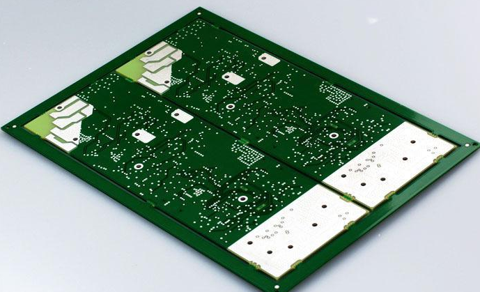
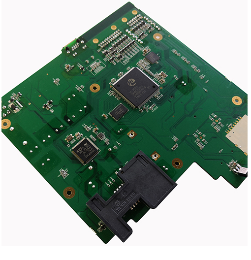
Patch processing
The PCBA processing no-clean welding process is not only suitable for the welding of through-hole plug-in components, hybrid assembly components and full-surface assembly components, but also for the assembly of multi-lead fine-pitch components. The following advantages are shown in these applications.
(1) It is used in dual wave soldering process. Because flux is used less or not, soldering defects caused by flux gas are eliminated, nozzle clogging is eliminated, and the stability of wave soldering is improved, which is conducive to obtaining high quality Welding connection.
(2) The cleaning process and corresponding equipment are eliminated, which greatly reduces the operating cost.
(3) Since the oxidation of the solder and the soldering part is eliminated, the wettability of the solder and the solderability of the soldering part are improved, thereby minimizing soldering defects, greatly improving the soldering quality, and ensuring the soldering reliability of the components .
Therefore, PCBA processing no-clean welding technology is a very valuable practical technology, and its promotion and application have very important practical significance in terms of technology, economic benefits and protection of the human living environment.
iPCB is happy to be your business partner. Our business goal is to become the most professional prototyping PCB manufacturer in the world. With more than ten years of experience in this field, we are committed to meeting the needs of customers from different industries in terms of quality, delivery, cost-effectiveness and any other demanding requirements. As one of the most experienced PCB manufacturers and SMT assemblers in China, we are proud to be your best business partner and good friend in all aspects of your PCB needs. We strive to make your research and development work easy and worry-free.
quality assurance
iPCB has passed ISO9001:2008, ISO14001, UL, CQC and other quality management system certifications, produces standardized and qualified PCB products, masters complex process technology, and uses professional equipment such as AOI and Flying Probe to control production and X-ray inspection machines. Finally, we will use double FQC inspection of appearance to ensure shipment under IPC II standard or IPC III standard.