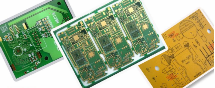
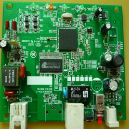
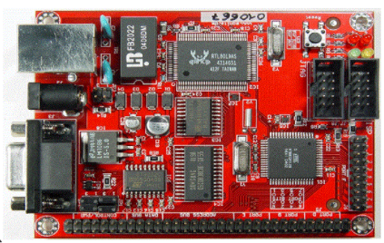
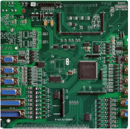
1. Layout
First, consider the PCB size. When the PCB size is too large, the printed lines will be long, the impedance will increase, the anti-noise ability will decrease, and the cost will also increase; if the PCB size is too small, the heat dissipation will not be good, and adjacent lines will be easily disturbed. After determining the PCB size, determine the location of the special components. Finally, according to the functional units of the circuit, all the components of the circuit are laid out.

The following principles should be observed when determining the location of special components:
(1) Shorten the wiring between high-frequency components as much as possible, try to reduce their distribution parameters and mutual electromagnetic interference. Components that are susceptible to interference should not be too close to each other, and input and output components should be kept as far away as possible.
(2) There may be a high potential difference between some components or wires, and the distance between them should be increased to avoid accidental short circuits caused by discharge. The components with high voltage should be arranged as far as possible in places that are not easily reachable by hands during debugging.
(3) The position occupied by the positioning hole of the printed board and the fixed bracket should be reserved.
According to the functional unit of the circuit. When laying out all the components of the circuit, the following principles must be met:
(1) Arrange the position of each functional circuit unit according to the circuit flow, so that the layout is convenient for signal circulation, and the signal is kept in the same direction as possible.
(2) Take the core component of each functional circuit as the center and lay out around it. The components should be evenly, neatly and compactly arranged on the PCB. Minimize and shorten the leads and connections between the components.
(3) For circuits operating at high frequencies, the distributed parameters between components must be considered. Generally, the circuit should be arranged in parallel as much as possible. In this way, it is not only beautiful, but also easy to install and weld. It is easy to mass produce.
(4) The components located at the edge of the circuit board are generally not less than 2mm away from the edge of the circuit board. The best shape of the circuit board is rectangular. The aspect ratio is 3:2 to 4:3. When the size of the circuit board is larger than 200x150mm, the mechanical strength of the circuit board should be considered.
2. Wiring
The principles of wiring are as follows:
(1) The wires used for the input and output terminals should try to avoid being adjacent and parallel. It is best to add ground wires between wires to avoid feedback coupling.
(2) The minimum width of the printed wire is mainly determined by the adhesion strength between the wire and the insulating substrate and the current value flowing through them.
(3) The corners of the printed conductors are generally arc-shaped, and the right angle or the included angle will affect the electrical performance in the high-frequency circuit. In addition, try to avoid using large-area copper foil, otherwise the copper foil will expand and fall off when heated for a long time. When a large-area copper foil is required, it is best to use a grid shape. This will help to eliminate the volatile gas generated by the heating of the adhesive between the copper foil and the substrate.
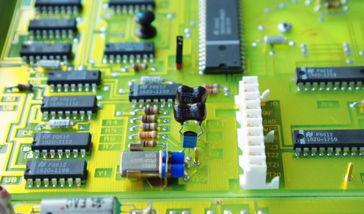
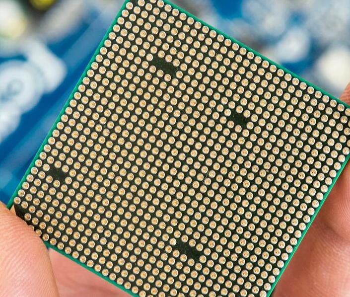
3. Pad
The center hole of the pad (in-line device) is slightly larger than the diameter of the device lead. If the pad is too large, it is easy to form a false solder. The outer diameter D of the pad is generally not less than (d+1.2) mm, where d is the lead diameter. For high-density digital circuits, the minimum diameter of the pad can be (d+1.0) mm.
PCB and circuit anti-interference measures:
The anti-jamming design of the printed circuit board has a close relationship with the specific circuit. Here, only a few common measures of PCB anti-jamming design are explained.
1. Power cord design
According to the size of the printed circuit board current, try to increase the width of the power line to reduce the loop resistance. At the same time, make the direction of the power line and ground line consistent with the direction of data transmission, which helps to enhance the anti-noise ability.
2. Lot design
The principles of ground wire design are:
(1) The digital ground is separated from the analog ground. If there are both logic circuits and linear circuits on the circuit board, they should be separated as much as possible. The ground of the low-frequency circuit should be grounded in parallel at a single point as much as possible. When the actual wiring is difficult, it can be partially connected in series and then grounded in parallel. The high-frequency circuit should be grounded at multiple points in series, the ground wire should be short and leased, and the grid-like large-area ground foil should be used around the high-frequency component as much as possible.
(2) The grounding wire should be as thick as possible. If the ground wire uses a very tight line, the ground potential changes with the change of the current, which reduces the anti-noise performance. Therefore, the ground wire should be thickened so that it can pass three times the allowable current on the printed board. If possible, the grounding wire should be 2~3mm or more.
(3) The ground wire forms a closed loop. For printed boards composed only of digital circuits, most of their grounding circuits are arranged in loops to improve noise resistance.
4. Decoupling capacitor configuration
One of the conventional methods of PCB design is to configure appropriate decoupling capacitors on each key part of the printed board. The general configuration principles of decoupling capacitors are:
(1) Connect a 10~100uf electrolytic capacitor across the power input. If possible, it is better to connect to 100uF or more.
(2) In principle, each integrated circuit chip should be equipped with a 0.01uf~0.1uf ceramic capacitor. If the gap of the printed board is not enough, a 1~10pF capacitor can be arranged for every 4~8 chips.
(3) For devices with weak anti-noise ability and large power changes when shutting down, such as RAM and ROM storage devices, a decoupling capacitor should be directly connected between the power line and the ground line of the chip.
5. Via design
In high-speed PCB design, seemingly simple vias will often bring great negative effects to the design of the circuit. In order to reduce the adverse effects caused by the parasitic effects of vias, we can do our best in the design.
(1) Considering both cost and signal quality, choose a reasonable size via size. For example, for the 6-10 layer memory module PCB design, it is better to use 10/20mil (drilled/pad) vias. For some high-density small-size boards, you can also try to use 8/18mil vias. hole. Under current technical conditions, it is difficult to use smaller-sized vias (when the depth of the hole exceeds 6 times the diameter of the drilled hole, it is impossible to ensure that the hole wall can be evenly plated with copper); for the power or ground vias, Consider using a larger size to reduce impedance.
(2) Try not to change the layers of the signal traces on the PCB board, that is, try not to use unnecessary vias.
(3) The pins of the power supply and the ground should be punched nearby, and the lead between the via and the pin should be as short as possible
(4) Place some grounded vias near the vias of the signal change layer to provide the nearest loop for the signal. It is even possible to place a large number of redundant ground vias on the PCB board.
6. Some experience in reducing noise and electromagnetic interference
(1) Low-speed chips can be used instead of high-speed chips. High-speed chips are used in key places
(2) A resistor can be used in series to reduce the jump rate of the upper and lower edges of the control circuit.
(3) Try to provide some form of damping for relays, such as RC setting current damping
(4) Use the lowest frequency clock that meets the system requirements.
(5) The clock should be as close as possible to the device using the clock. The shell of the quartz crystal oscillator should be grounded. The clock area should be circled with a ground wire. The clock wire should be as short as possible. Do not run wires under the quartz crystal or under noise-sensitive devices. The clock, bus, and chip select signals should be far away from the I/O lines and connectors.The clock line perpendicular to the I/O line has less interference than the parallel to the I/O line.
(6) Do not leave the input terminal of the gate circuit that is not in use. The positive input terminal of the unused op amp is grounded, and the negative input terminal is connected to the output terminal.