Printed circuit boards are considered to be the key to electronic products currently available on the market. In the case of a small tool for calculations, even if there is something necessary, such as a digital clock-there is probably a PCBA in it. PCBA, inject vitality into gadgets by controlling electronic signs, because they must meet the electronic needs of gadgets.
In order to achieve this, the circuit board is composed of a series of methods that need to be adhered. Copper vias enable the circuit board to provide direct current to all parts of the PCBA. Three kinds of PCBAs are manufactured. Therefore, it is important to understand the comparison between them so that you can choose the right PCBA that meets your needs. In order to better understand the function of PCBA, we will stroll to how to make PCBA so that you can become a PCBA buyer.
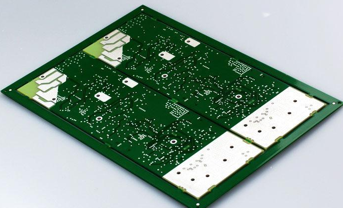
PCBA manufacturing
The main steps of PCBA manufacturing are as follows:

PCBAShopper-Develop PCBA design
To start the PCBA manufacturing process, you must first make a plan. The most commonly used design software used by PCBA architects is called ExtendedGerber, also known as IX274X. Regarding PCBA configuration, ExtendedGerber is a great programming because it also plays the role of output design. This extension Gerber converts all data in the encoded form required by the initiator.
PCBAShopper-pre-bonded copper used in the inner layer
The third step becomes the initial stage of circuit board manufacturing. Once the PCBA design is laminated, the manufacturer must pre-adhere it to the laminate as a structural filling for the circuit board. The manufacturer then removes the copper to reveal the previous diagram. Next, the cover plate is fixed by a beautiful photo film called resist. This element enables experts to obtain the ideal combination of chart photos and photoresist printing materials.
PCBAShopper-inspection and layer alignment
Optical inspection and correctness are very necessary, because once the layers are aligned and laminated, any existing errors cannot be corrected.
PCBAShopper-drilling
When preparing to drill the PCBA, use the X-ray machine to find the drilling point. At this point, you should first make pilot holes to fix the circuit board stack, and then drill more holes. Regarding penetrating these bits, use computer-based grids in the boreholes and use the extended Gerber program to provide guidance. When finished, any excess copper left on the surface will be scraped off.
PCBAShopper-PCBA electroplating
Learn about flexible PCBA materials.
Place the flexible layer in the center of the stack to protect the outer layer. The electroplating process uses synthetic materials to fuse the PCBA layers together. After cleaning, the circuit board will be soaked with chemicals.
Last etch
Regarding the etching of the outer layer of PCBA, tin protection is used during the etching process to help ensure copper. When all the unwanted copper has been evacuated, the PCBA association has been properly established and is ready for solder mask.
in conclusion
Other steps include applying solder mask, completing PCBA and silk screen, electrical reliability testing, and finally cutting and analyzing. From the manufacturer's point of view, these further steps are essential, and do not have to be described in detail for PCBA shoppers. A correct understanding of the above process will definitely convince you as a shopper to decide and buy PCBA when you think it is necessary.